Semiconductor device and method for manufacturing thereof
- Summary
- Abstract
- Description
- Claims
- Application Information
AI Technical Summary
Benefits of technology
Problems solved by technology
Method used
Image
Examples
Embodiment Construction
[0020] An embodiment of the present invention will now be described with reference to accompanying drawings.
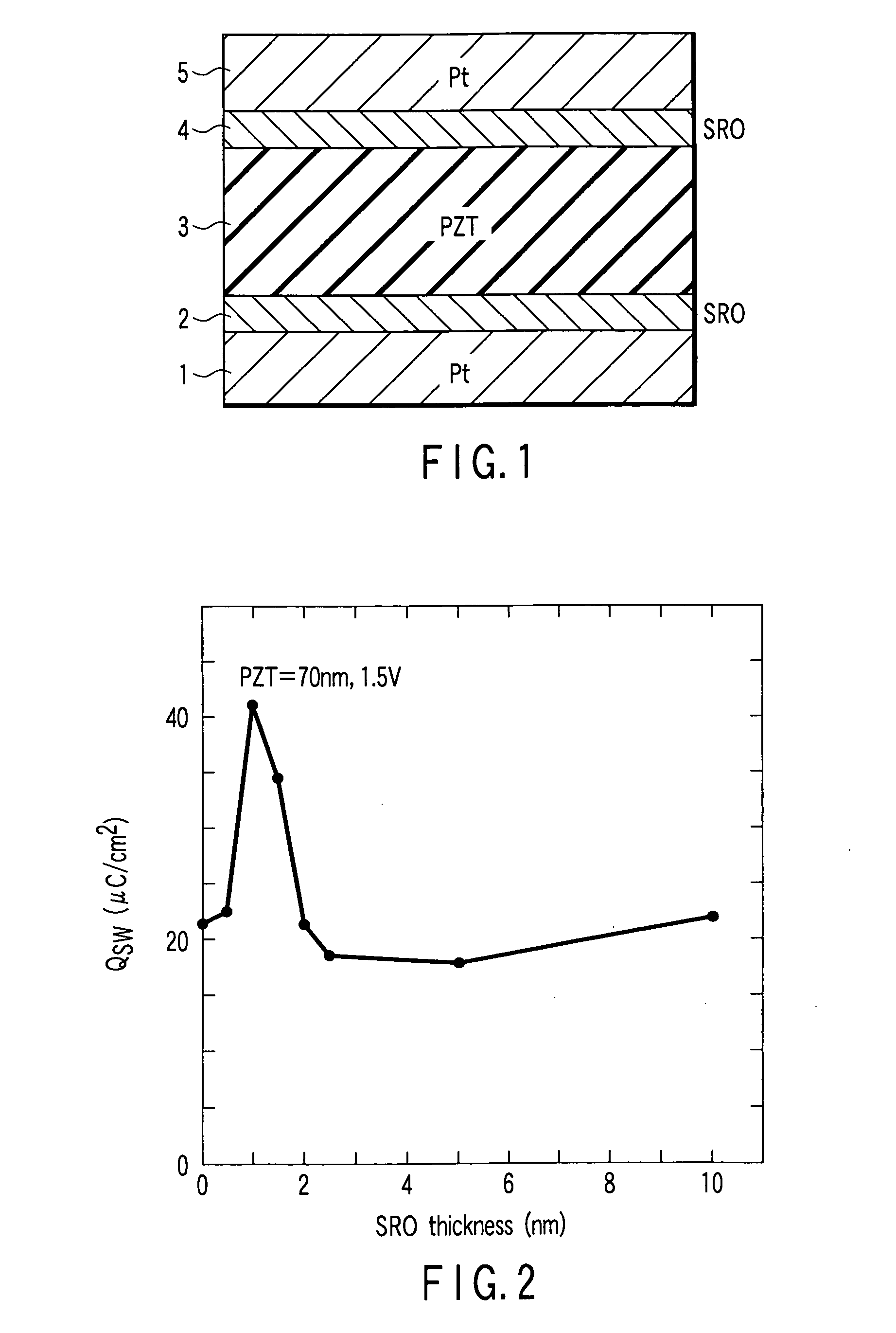
[0021] The inventor of the present invention discovered that when a PZT film is formed on a conventional lower SRO electrode, PZT is randomly oriented. The inventor further found that the cause that a sufficient polarization amount cannot be obtained in the conventional capacitor resides in the random orientation of PZT. Under the circumstances, the invention carried out intensive studies focusing on the orientation of PZT and has found that PZT can be made to have a desired orientation, more specifically, a priority orientation of (111) by setting the thickness of the lower SRO film to 2 nm or less. Based on this finding, the present invention has been achieved.
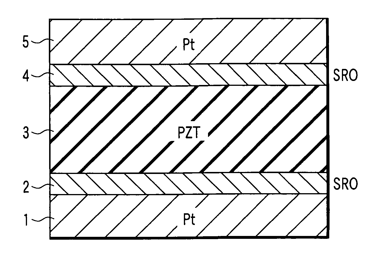
[0022]FIG. 1 is a schematic diagram showing the layer structure of a semiconductor device according to an embodiment of the present invention. The semiconductor device shown in this figure is a capacitor that employs...
PUM
 Abstract
Description
Claims
Application Information


