Image pickup system for preventing image darkening due to the entrance of intense light

a pickup system and pickup technology, applied in the field of image pickup system, can solve the problems of image darkening, change in output voltage at the reset, image darkening, etc., and achieve the effect of shortening the time required for judgment and processing

Inactive Publication Date: 2005-10-13
PANASONIC CORP
View PDF6 Cites 26 Cited by
  • Summary
  • Abstract
  • Description
  • Claims
  • Application Information

AI Technical Summary

Benefits of technology

[0039] Since the present invention requires conducting judgments and processing based on the read voltages in advance, the time re

Problems solved by technology

Although having excellent characteristics such as a low noise level, amplified image sensors have a problem that images are subject to darkening due to the entrance of intense light.
However, the change in output voltages at the reset is the very cause leading to image darkening, and has a direct effect on luminance information even if the amount of the change is small.
However, the change in output voltages at the reset cannot be de

Method used


Image

  • Image pickup system for preventing image darkening due to the entrance of intense light
  • Image pickup system for preventing image darkening due to the entrance of intense light
  • Image pickup system for preventing image darkening due to the entrance of intense light

Examples


first embodiment

1. First Embodiment

1.1 Structure

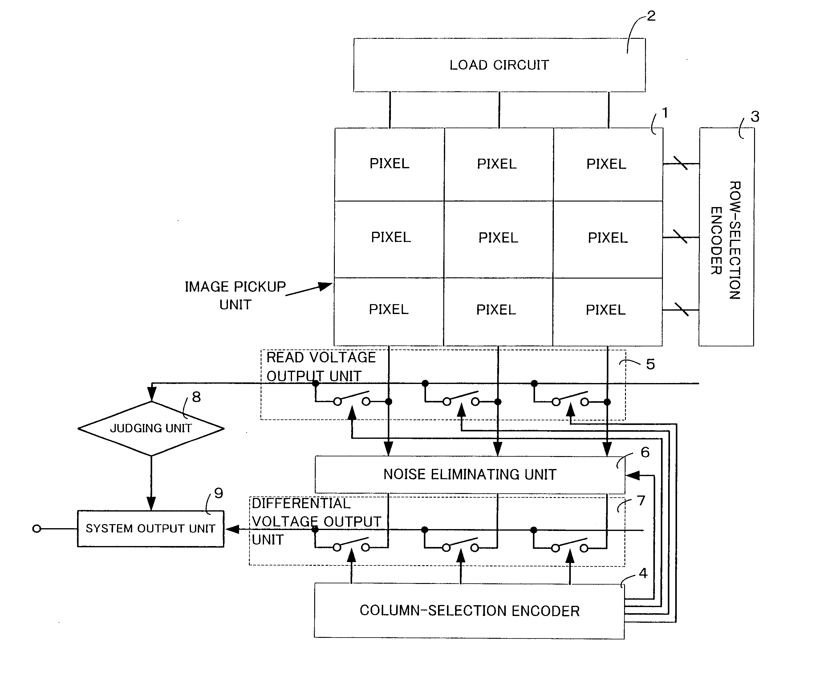
[0060]FIG. 1 shows a schematic structure of an image pickup apparatus according to a first embodiment of the present invention.

[0061] As shown in FIG. 1, the image pickup apparatus of the first embodiment comprises: an image pickup unit 1, a load circuit 2, a row-selection encoder 3, a column-selection encoder 4, a read voltage output unit 5, a noise eliminating unit 6, a differential voltage output unit 7, a judging unit 8, and a system output unit 9.

[0062] The image pickup unit 1 is an image pickup area in which a plurality of unit cells are arranged in a one- or two-dimensional array. Here, the structure of the first embodiment is described, using an example of the image pickup unit 1 composed of nine pixels arranged in a two-dimensional matrix of 3 rows by 3 columns. However, the actual number of pixels structuring the image pickup unit 1 is thousands in the case of a one-dimensional array, and hundreds of thousand to millions in the case of a...

second embodiment

2. Second Embodiment

2.1 Structure

[0096]FIG. 7 shows a schematic structure of an image pickup apparatus according to a second embodiment of the present invention.

[0097] As shown in FIG. 7, the image pickup apparatus of the second embodiment comprises: an image pickup unit 1, a load circuit 2, a row-selection encoder 3, a column-selection encoder 4, a read voltage output unit 5, a noise eliminating unit 6, a differential voltage output unit 7, a judging unit 8, a selecting unit 10, and a system output unit 11.

[0098] Note that the same numbers are used for the same components as in the first embodiment, and their descriptions are omitted.

[0099] The selecting unit 10 selects, based on the differential voltages outputted from the differential voltage output unit 7, unit cells targeted for correction from among unit cells whose read voltages have been judged by the judging unit 8 as not being within the predetermined range.

[0100]FIG. 8 shows a detailed structure of the selecting uni...

first modification

3. First Modification

[0126] In semiconductor image pickup devices such as CMOS sensors, the noise eliminating unit is generally provided on one side of the image pickup unit, and therefore the optical center is out of alignment with the chip center.

[0127] As compared to a conventional semiconductor image pickup device, switching devices such as transistors, capacity devices such as condensers, amplifier circuits and the like are added on to the semiconductor image pickup device of the present invention in order to output read voltages.

[0128] Given this factor, a first modification of the present invention involves reducing the misalignment between the optical center and chip center by positioning symmetrically the additional components used for the read voltage output to the differential voltage output unit with a center at the image pickup unit.

3.1 Structure

[0129]FIG. 10 shows a schematic structure of an image pickup apparatus according to the first modification of the present...


PUM


Abstract

The image pickup device comprises: an image pickup unit 1 in which a plurality of unit cells for generating reset and read voltages are arranged; a noise eliminating unit 6 for generating, with respect to each unit cell, a differential voltage corresponding to a difference between the reset and read voltages; and output units 5 and 7 for outputting the read and differential voltages, respectively, to a signal processing apparatus. The signal processing apparatus comprises: a judging unit 8 for judging whether each of the read voltages is within a predetermined range; and a system output unit 9 for outputting, for unit cells whose voltages are judged as being within the predetermined range, corresponding differential voltages as luminance information of the unit cells; for unit cells whose voltages are judged as not being within the predetermined range, a predetermined voltage indicating high luminance as luminance information of the unit cells.

Description

BACKGROUND OF THE INVENTION [0001] [1] Field of the Invention [0002] The present invention relates to an image pickup system in which a plurality of unit cells each performing photoelectric conversion on light incident thereto are arranged on a semiconductor substrate in a one- or two-dimensional array, in particular to a technology for preventing a phenomenon that images become dark due to the entrance of intense light. [0003] [2] Description of the Related Art [0004] Late years, image pickup systems using an image pickup apparatus are commonly used, and representative examples of such image pickup systems are home video cameras and digital still cameras. [0005] Some of these image pickup systems have an amplified image sensor as the image pickup apparatus. [0006] Although having excellent characteristics such as a low noise level, amplified image sensors have a problem that images are subject to darkening due to the entrance of intense light. [0007] In Japanese Laid-Open Patent Ap...

Claims


Application Information

Patent Timeline
IPC IPC(8): H04N5/235H04N5/335H04N5/355H04N5/374H01L27/146H04N5/376H04N5/378
CPCH04N5/3598H04N5/235H04N23/70H04N25/627A01B13/08A01B59/042A01B27/00
Inventor MASUYAMA, MASAYUKIMATSUNAGA, YOSHIYUKIMURAKAMI, MASASHI
Owner PANASONIC CORP
Why Eureka
Try Eureka