Nanowire light emitting device and method of fabricating the same
- Summary
- Abstract
- Description
- Claims
- Application Information
AI Technical Summary
Benefits of technology
Problems solved by technology
Method used
Image
Examples
Embodiment Construction
[0025] A nanowire light emitting device and a method of fabricating the same according to the present invention will become more apparent by describing in detail exemplary embodiments thereof with reference to the attached drawings. Throughout the drawings, like reference numerals refer to like elements, and their descriptions will not be repeated.
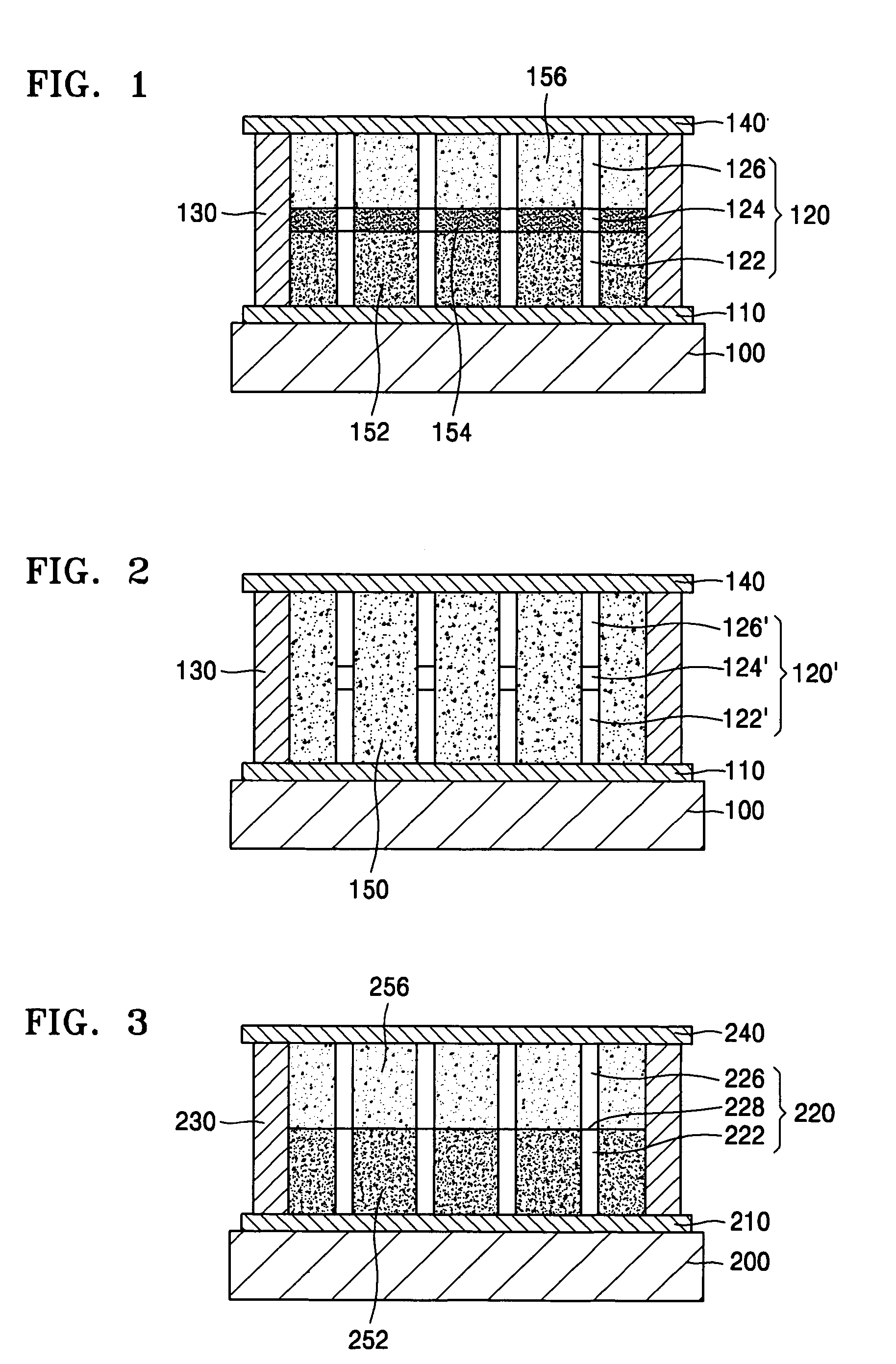
[0026]FIG. 1 is a cross-sectional view of a nanowire light emitting device according to a first exemplary embodiment of the present invention.
[0027] Referring to FIG. 1, a conductive layer (a first electrode layer) 110 is formed on a substrate 100 and a plurality of nanowires 120 are vertically formed on the conductive layer 110. A second electrode layer 140 is formed on the nanowires 120. A wall frame 130 is interposed between the first conductive layer 110 and the second conductive layer 140 and seals the space where the nanowires 120 are formed.
[0028] The nanowires 120 each have a p-type doped portion 122, an n-type doped portion 126...
PUM
| Property | Measurement | Unit |
|---|---|---|
| Polarity | aaaaa | aaaaa |
| Electrical conductor | aaaaa | aaaaa |
| Affinity | aaaaa | aaaaa |
Abstract
Description
Claims
Application Information


