Display drive device and drive controlling method
a technology of a display panel and a control method, which is applied in the direction of instruments, computing, electric digital data processing, etc., can solve the problems of insufficient control of the stick of liquid crystal molecules and the like, and achieve the effect of improving the display quality and the longevity life of the display panel
- Summary
- Abstract
- Description
- Claims
- Application Information
AI Technical Summary
Benefits of technology
Problems solved by technology
Method used
Image

Examples
first embodiment
[0051] Next, the data driver (display drive device) concerning this invention will be explained with reference to the drawings.
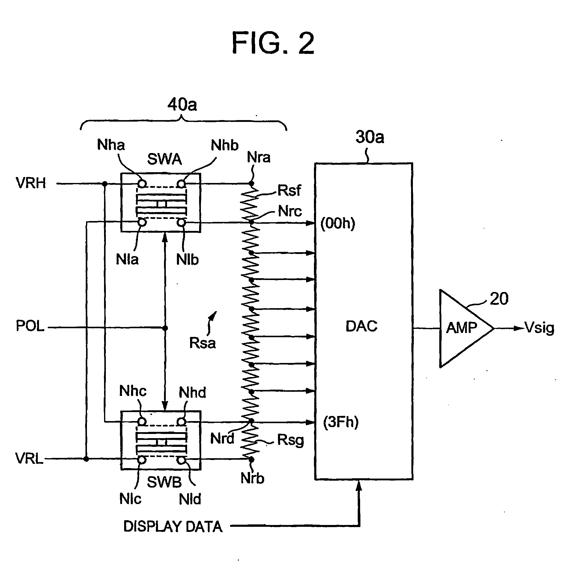
[0052]FIG. 2 is an outline block diagram showing the first embodiment section concerning the output of the display signal voltage of the data driver related this invention.
[0053]FIGS. 3A and 3B are conceptual diagrams showing an operating state of the data driver concerning this embodiment.
[0054]FIG. 4 is a characteristic drawing showing an example of the relationship of the output level (display signal voltage) to the input data (luminosity gradations) of the data driver concerning the first embodiment.
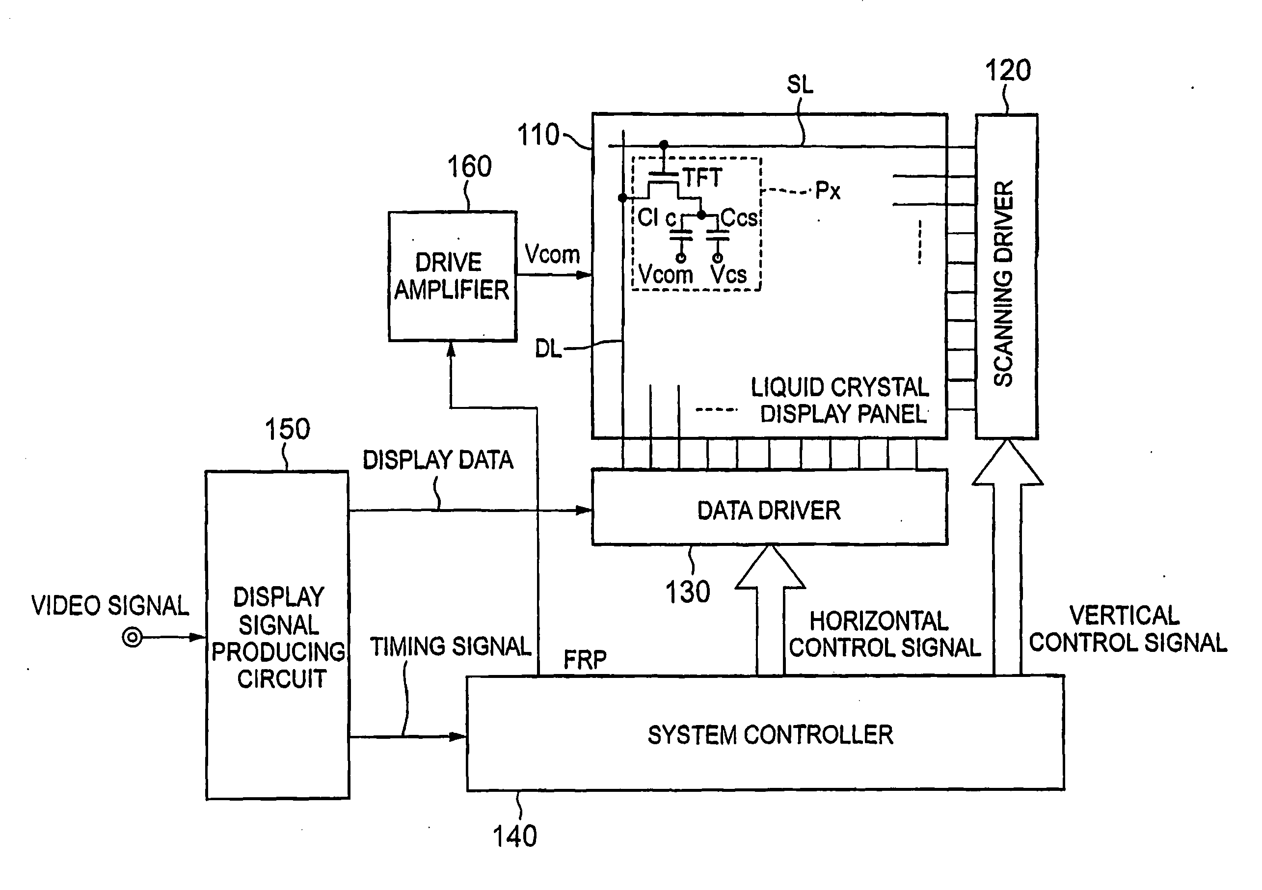
[0055] In addition, with regard to any configuration equivalent (FIG. 13) of the conventional technology mentioned above, the same or equivalent nomenclature is appended to simplify the explanation. Also, explanation will refer accordingly to the configuration (FIG. 1) of the display device mentioned above.
[0056] As shown in FIG. 2, the data driver (displ...
second embodiment
[0079] Subsequently, the data driver (display drive device) concerning this invention will be explained with reference to the drawings.
[0080] As the data driver applicable to the display device concerning this invention in the first embodiment mentioned above, although the case comprising the changeover switches SWA and SWB which suitably switches and controls these changeover switches SWA, SWB based on the polarity changeover signal POL; has a configuration which switches and sets the reference voltage VRH by the high potential side, the reference voltage VRL by the low potential side, and a connecting location with the division resistance Rsa; sets to one side of the signal polarity of the display signal voltage Vsig (gradation voltage); set the reference voltage which regulates the highest gradation and lowest gradation that increases and decreases by predetermined correction voltage respectively from the reference voltage VRH by the high potential side and the reference voltage ...
third embodiment
[0087] Next, the data driver (display drive device) concerning this invention will be explained with reference to the drawings.
[0088]FIG. 9 is an outline block diagram showing the third embodiment of the section concerning the output of the display signal voltage of the data driver concerning this invention.
[0089]FIGS. 10A and 10B are conceptual diagrams showing an operating state of the data driver concerning the third embodiment.
[0090]FIG. 11 is a characteristic drawing showing an example of the relationship of the output level (display signal voltage) to the input data (luminosity gradations) of the data driver concerning the third embodiment.
[0091] Here, concerning any configuration equivalent to each embodiment mentioned above, the same or equivalent nomenclature is appended and the explanation is simplified or omitted from the description.
[0092] As shown in FIGS. 10A and 10B, the data driver related to this embodiment, for example, comprises a gradation voltage setting cir...
PUM
| Property | Measurement | Unit |
|---|---|---|
| luminosity | aaaaa | aaaaa |
| voltage range | aaaaa | aaaaa |
| display signal voltage | aaaaa | aaaaa |
Abstract
Description
Claims
Application Information
 - R&D
- Intellectual Property
- Life Sciences
- Materials
- Tech Scout
- Unparalleled Data Quality
- Higher Quality Content
- 60% Fewer Hallucinations
Browse by: Latest US Patents, China's latest patents, Technical Efficacy Thesaurus, Application Domain, Technology Topic, Popular Technical Reports.
© 2025 PatSnap. All rights reserved.Legal|Privacy policy|Modern Slavery Act Transparency Statement|Sitemap|About US| Contact US: help@patsnap.com