Semiconductor memory device

a memory device and semiconductor technology, applied in the field of semiconductor memory devices, can solve the problems of difficult to flexibly use the timing margin of trfc, and achieve the effects of reducing the probability of failure, and improving the yield of products upon tes

Active Publication Date: 2005-10-20
SK HYNIX INC
View PDF5 Cites 74 Cited by
  • Summary
  • Abstract
  • Description
  • Claims
  • Application Information

AI Technical Summary

Benefits of technology

[0005] Accordingly, the present invention has been made in view of the above problems, and it is an object of the present invention to provide a control circuit of a semiconductor...

Problems solved by technology

At this time, since tRC and tRFC use the same tRAS_min delay ...

Method used


Image

  • Semiconductor memory device
  • Semiconductor memory device
  • Semiconductor memory device

Examples


Embodiment Construction

[0016] Now, the preferred embodiments according to the present invention will be described with reference to the accompanying drawings.

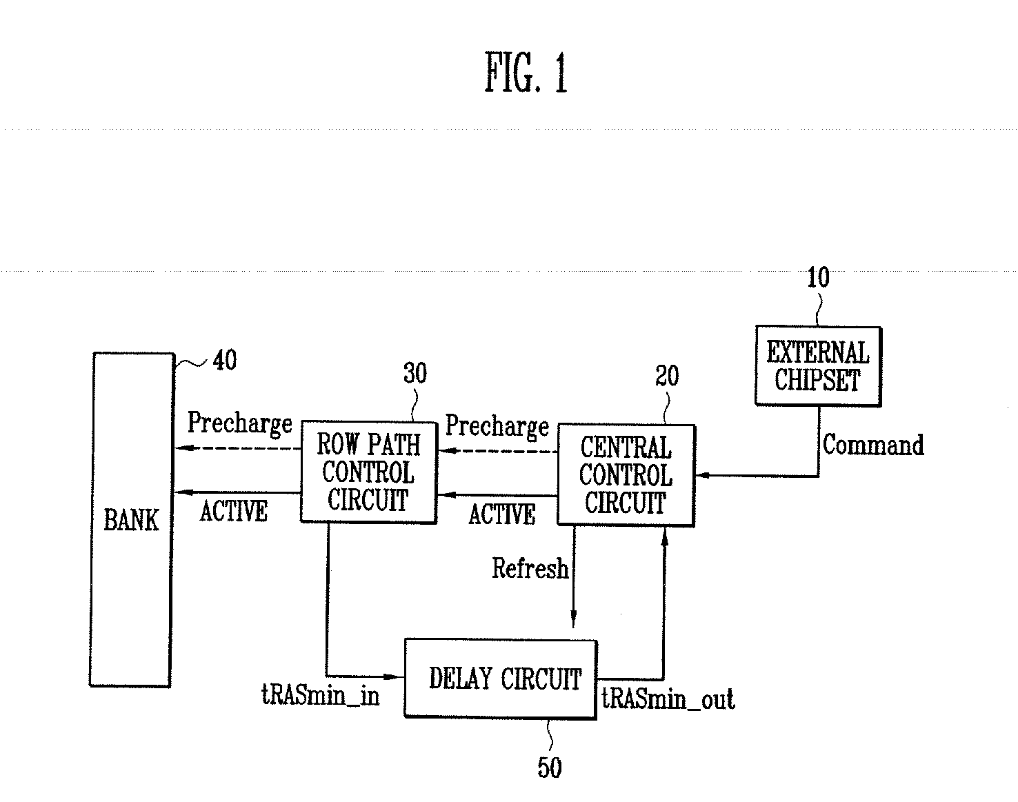
[0017]FIG. 1 is a block diagram illustrating the construction of a control circuit of a semiconductor memory device according to the present invention.

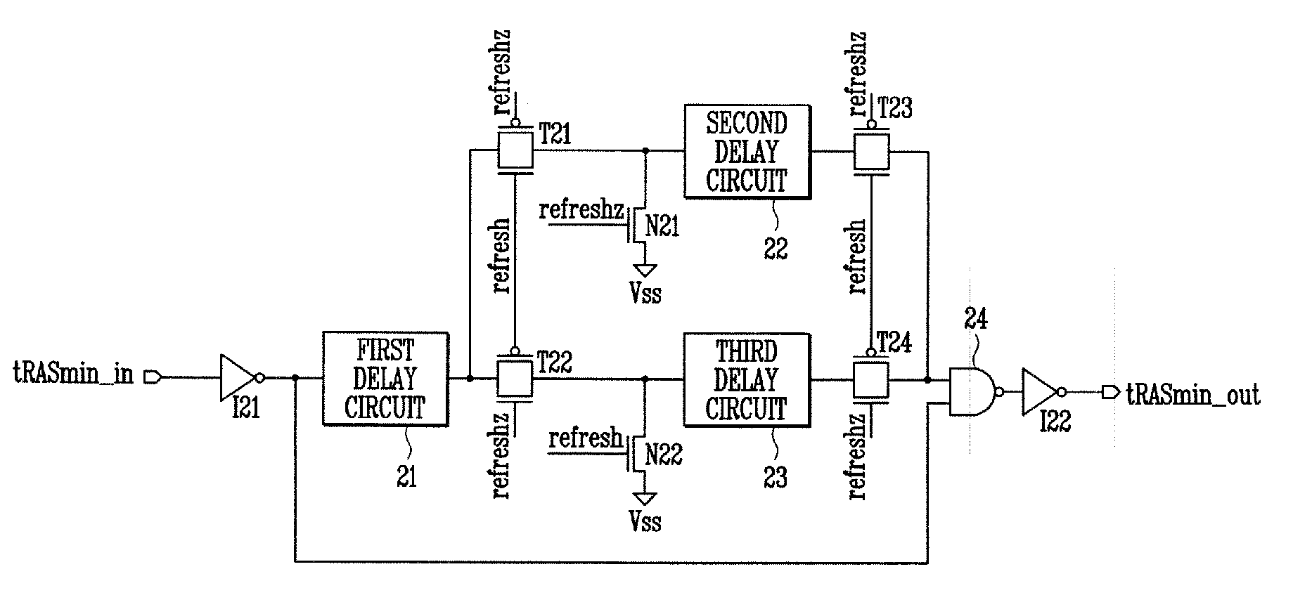
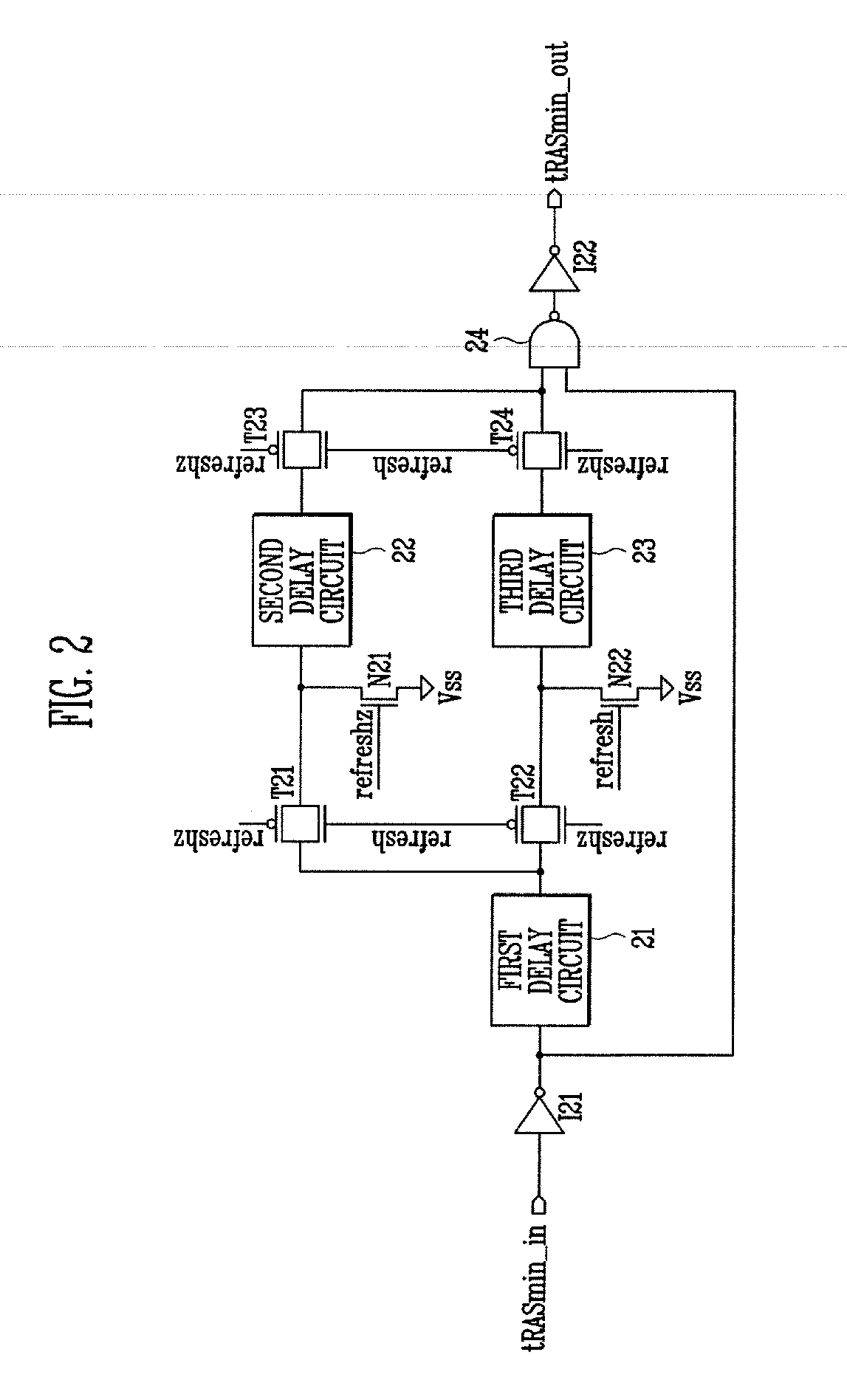
[0018] If a command such as write with auto-precharge, read with auto-precharge or auto-refresh is applied from an external chipset 10, a central control circuit 20 of a DRAM applies an active signal ACTIVE for executing this command to a row path control circuit 30. The row path control circuit 30 inputs a control signal tRASmin_in to a delay circuit 50 while applying the active signal ACTIVE to a bank 40. The delay circuit 50 having a delay time, which has been suitably tuned to tRAS_min, delays the control signal tRASmin_in for a predetermined time and outputs a delay signal tRASmin_out to the central control circuit 20. The central control circuit 20 generates a precharge signal Precharge and inp...


PUM


Abstract

The present invention relates to a semiconductor memory device. According to the present invention, a delay circuit is constructed in order for a refresh operation and a normal operation to have different delay paths such that a minimum tRAS (Active to Precharge command period) delay time of the refresh operation to which tRFC (Auto Referesh to Active/Auto Referesh command period) is applied is longer than a minimum tRAS delay time of a normal operation to which tRC (Active to Active/Auto Refresh command period) is applied. Thus, a greater noise margin is secured in tRFC in a refresh operation being the worst situation of a DRAM. Accordingly, the probability that fail can occur is reduced and the yield upon test is thus improved.

Description

CROSS REFERENCE TO RELATED APPLICATIONS [0001] This application relies for priority upon Korean Patent Application No. 2004-0027093 filed Apr. 20, 2004, the contents of which are herein incorporated by reference in their entirety. FIELD OF THE INVENTION [0002] The present invention relates to a semiconductor memory device. More specifically, the present invention relates to a control circuit of a semiconductor memory device, wherein a greater noise margin is secured in tRFC in a refresh operation being the worst situation of a DRAM in such a manner that a delay circuit is constructed in order for a refresh operation and a normal operation to have different delay paths such that a minimum tRAS (Active to Precharge command period) delay time of the refresh operation to which tRFC (Auto Referesh to Active / Auto Referesh command period) is applied is longer than a minimum tRAS delay time of a normal operation to which tRC (Active to Active / Auto Refresh command period) is applied, whereby...

Claims


Application Information

Patent Timeline
IPC IPC(8): G11C7/00G11C11/401G11C11/406G11C11/4094G11C29/02
CPCG11C11/401G11C11/406G11C2211/4061G11C29/02G11C29/50012G11C11/4094E05D15/42E05C9/021E05Y2900/148E05Y2201/216
Inventor PARK, MUN PHIL
Owner SK HYNIX INC
Why Eureka
Try Eureka