
Three-dimensional interconnect resistance extraction using variational method

a three-dimensional interconnect and resistance extraction technology, applied in the field of three-dimensional interconnect resistance extraction in the integral circuit design process, can solve the problems of difficult calculation of the resistance of these complicated structures, design limits on metal density, and time delay due to interconnections as significant as that of logic gates, so as to achieve fast and accurate interconnect resistance solver

Inactive Publication Date: 2005-10-20
BELL SEMICON LLC
View PDF20 Cites 6 Cited by
  • Summary
  • Abstract
  • Description
  • Claims
  • Application Information

AI Technical Summary

Benefits of technology

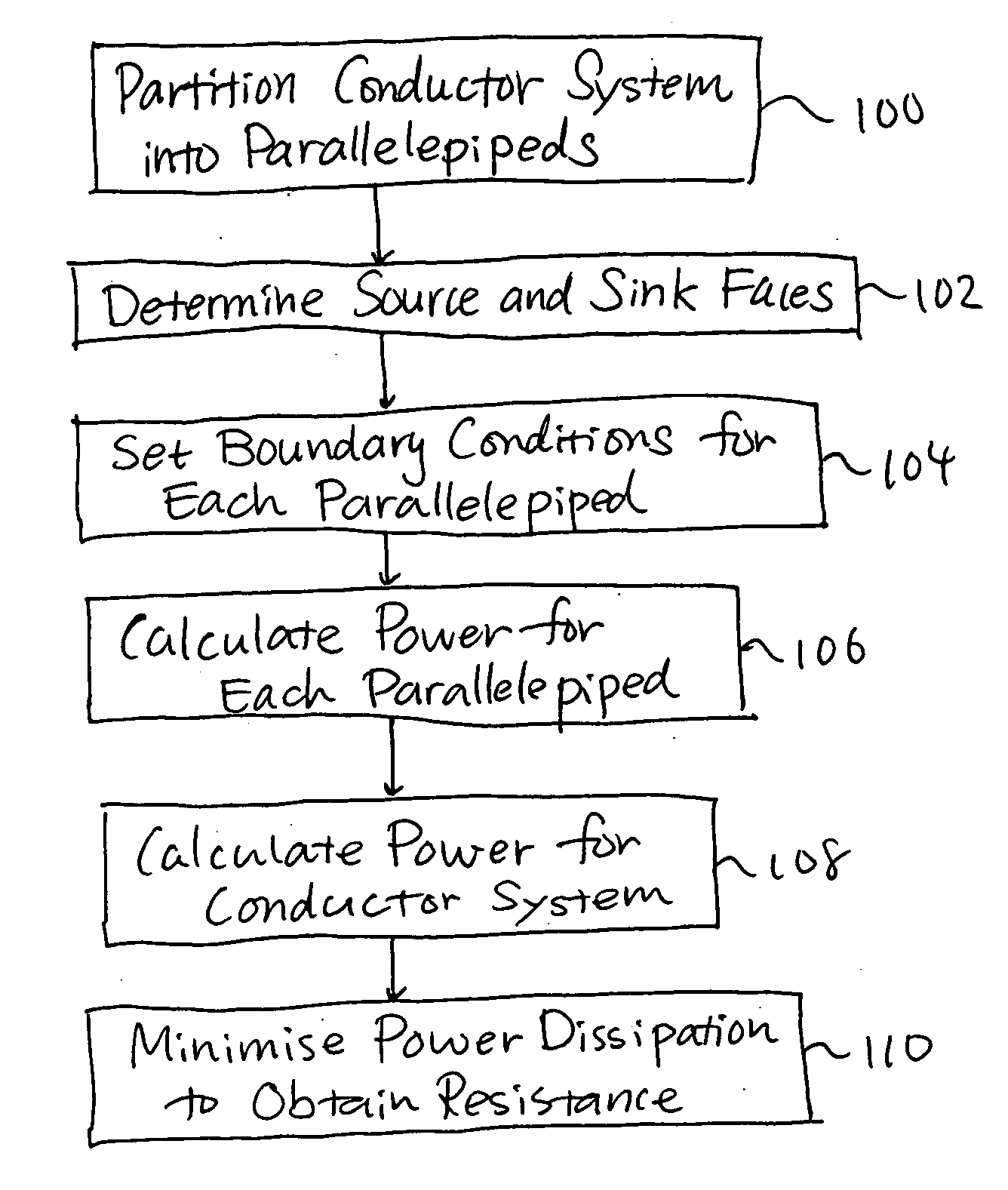
[0009] A method and apparatus calculate resistance of a conductor system for an integrated circuit design, the conductor system having a three-dimensional shape defined by boundary faces. The resistance calculation includes (a) partitioning the three-dimensional shape into a plurality of parallelepipeds, a boundary between two parallelepipeds forms an entire face for both of the two parallelepipeds, (b) determining at least one source face and at least one sink face from among the boundary faces, a current entering the conductor system through the source face and leaving the conductor system through the sink face, (c) setting boundary conditions with respect to the current for each of the parallelepipeds, (d) calculating power for each of the parallelepipeds with the boundary conditions, (e) calculating power for the conductor system based on the power and the boundary conditions of each of the parallelepipeds, and (f) obtaining the resistance of the conductor system by minimizing dissipation of the calculated power of the conductor system.

Problems solved by technology

As complexity and performance of IC and Very Large Scale Integration (VLSI) circuit increases, time delay due to interconnects is becoming as significant as that of logic gates.
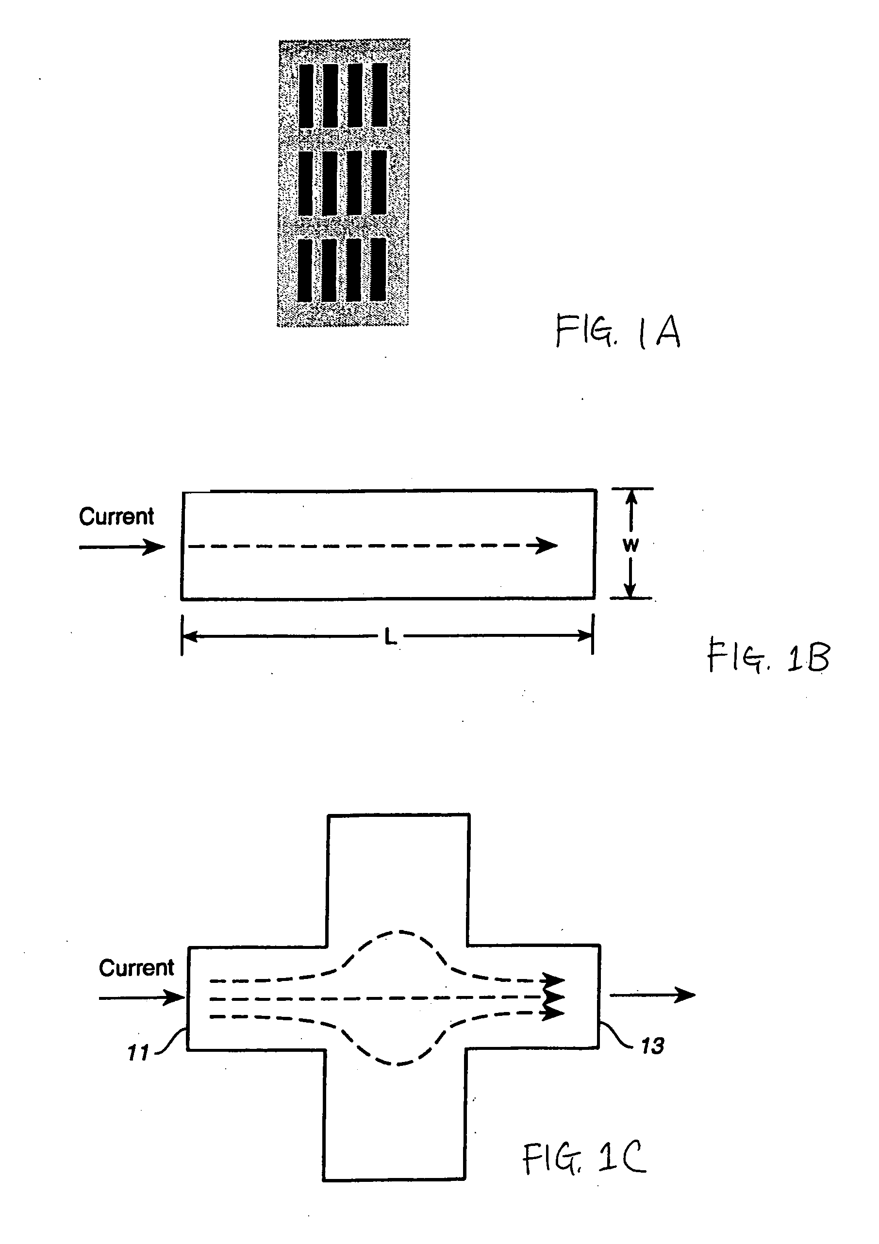
This leads to design limits on the metal density, and the introduction of nonmetal slots in large metal structures, such as wide metal lines as shown in FIG. 1A.
The resistance of these complicated structures is difficult to calculate.
However, conductor shapes can be more complicated, for example, as shown in FIG. 1C.
This makes it difficult to define a length and a width of the conductor shape, and renders the resistance calculation inaccurate.
However, this is not the case for interconnect resistance.
However, conformal transformations generally assume specific constant potential surfaces, which might not conform to the specific system at hand.
Moreover, this technique does not extend to three dimensions.

Method used


Image

  • Three-dimensional interconnect resistance extraction using variational method
  • Three-dimensional interconnect resistance extraction using variational method
  • Three-dimensional interconnect resistance extraction using variational method

Examples


Embodiment Construction

[0026] Embodiments of the present invention are described herein in the context of a three-dimensional interconnect resistance calculation using a variation al method. Those of ordinary skill in the art will realize that the following detailed description of the present invention is illustrative only and is not intended to be in any way limiting. Other embodiments of the present invention will readily suggest themselves to such skilled persons having the benefit of this disclosure. Reference will now be made in detail to implementations of the present invention as illustrated in the accompanying drawings. The same reference indicators will be used throughout the drawings and the following detailed description to refer to the same or like parts.

[0027] In the interest of clarity, not all of the routine features of the implementations described herein are shown and described. It will, of course, be appreciated that in the development of any such actual implementation, numerous impleme...


PUM


Abstract

A method and apparatus calculate resistance of a three-dimensional conductor system defined by boundary faces. The resistance calculation includes (a) partitioning the three-dimensional shape into a plurality of parallelepipeds, a boundary between two parallelepipeds forms and entire face for both of the two parallelepipeds, (b) determining at least one source face and at least one sink face from among the boundary faces, a current entering the conductor system through the source face and leaving the conductor system through the sink face, (c) setting boundary conditions with respect to the current for each of the parallelepipeds, (d) calculating power for each of the parallelepipeds with the boundary conditions, (e) calculating power for the conductor system based on the power and the boundary conditions of each of the parallelepipeds, and (f) obtaining the resistance of the conductor system by minimizing dissipation of the calculated power of the conductor system.

Description

CROSS REFERENCE TO RELATED APPLICATIONS OR PRIORITY CLAIM [0001] This application claims the benefit of provisional U.S. Patent Application Ser. No. 60 / 563,595 filed on Apr. 19, 2004 in the name of the same inventor. This application is also related to U.S. patent application Ser. No. 10 / 224,019, entitled “Calculating Resistance of Conductor Layer for Integrated Circuit Design,” filed on Aug. 19, 2002, in the name of the same inventor and commonly assigned to the same assignee, which is now U.S. Pat. No. 6,802,047 issued on Oct. 5, 2004.FIELD OF THE INVENTION [0002] The present invention relates to circuit extraction in integral circuit (IC) design processes. More particularly, the present invention relates to a method and apparatus for calculating resistance of a three-dimensional conductor system in an IC design. BACKGROUND OF THE INVENTION [0003] As complexity and performance of IC and Very Large Scale Integration (VLSI) circuit increases, time delay due to interconnects is becom...

Claims


Application Information

Patent Timeline
Patent Type & Authority Applications(United States)
IPC IPC(8): G06F17/50
CPCG06F17/5036G06F30/367
Inventor DONIGER, KENNETH
Owner BELL SEMICON LLC
Learn More