Masking circuit and method of masking corrupted bits

a masking circuit and corrupted bit technology, applied in the field of masking circuits and corrupted bits masking, can solve the problems of inability to repeat the output response, incorrect operation, and circuit described does not provide any means for handling defective scan chains, and achieve the effect of maximizing fault coverag

Inactive Publication Date: 2005-10-27
LOGICVISION
View PDF3 Cites 42 Cited by
  • Summary
  • Abstract
  • Description
  • Claims
  • Application Information

AI Technical Summary

Benefits of technology

[0016] These features allow at-speed production tests or field tests to be performed while maximizing fault coverage.

Problems solved by technology

However, there are circumstances where the output response is not completely predictable and repeatable and yet it is desired to compute a signature to analyze the part of the output response that is predictable and repeatable.
A non-repeatable output response can be caused by test patterns that are not valid functional patterns or by a design error or a defect.
Rather, they may be caused by incorrect operation of one or more scan chains.
The incorrect operation could be caused by a blockage of the scan data or scan data being lost because of a hold time problem.
The circuit described does not provide any means for handling defective scan chains or the loss of data caused by hold time problems.
The invention suffers from the drawback that the input and output mask controllers are relatively complex and require considerable circuit resources.
The drawbacks to this arrangement are that it focuses on diagnosis only and does not provide masking modes to maximize fault coverage in the presence of unknowns.
Also, the arrangement does not address problems associated with hold time which require to masking both scan chain inputs and scan chain outputs.

Method used


Image

  • Masking circuit and method of masking corrupted bits
  • Masking circuit and method of masking corrupted bits
  • Masking circuit and method of masking corrupted bits

Examples


Embodiment Construction

[0024] In the following detailed description, numerous specific details are set forth in order to provide a thorough understanding of the present invention, However, it will be understood by those skilled in the art that the present invention may be practiced without these specific details. In other instances, well known methods, procedures, components and circuits have not been described in detail so as not to obscure aspects of the present invention.

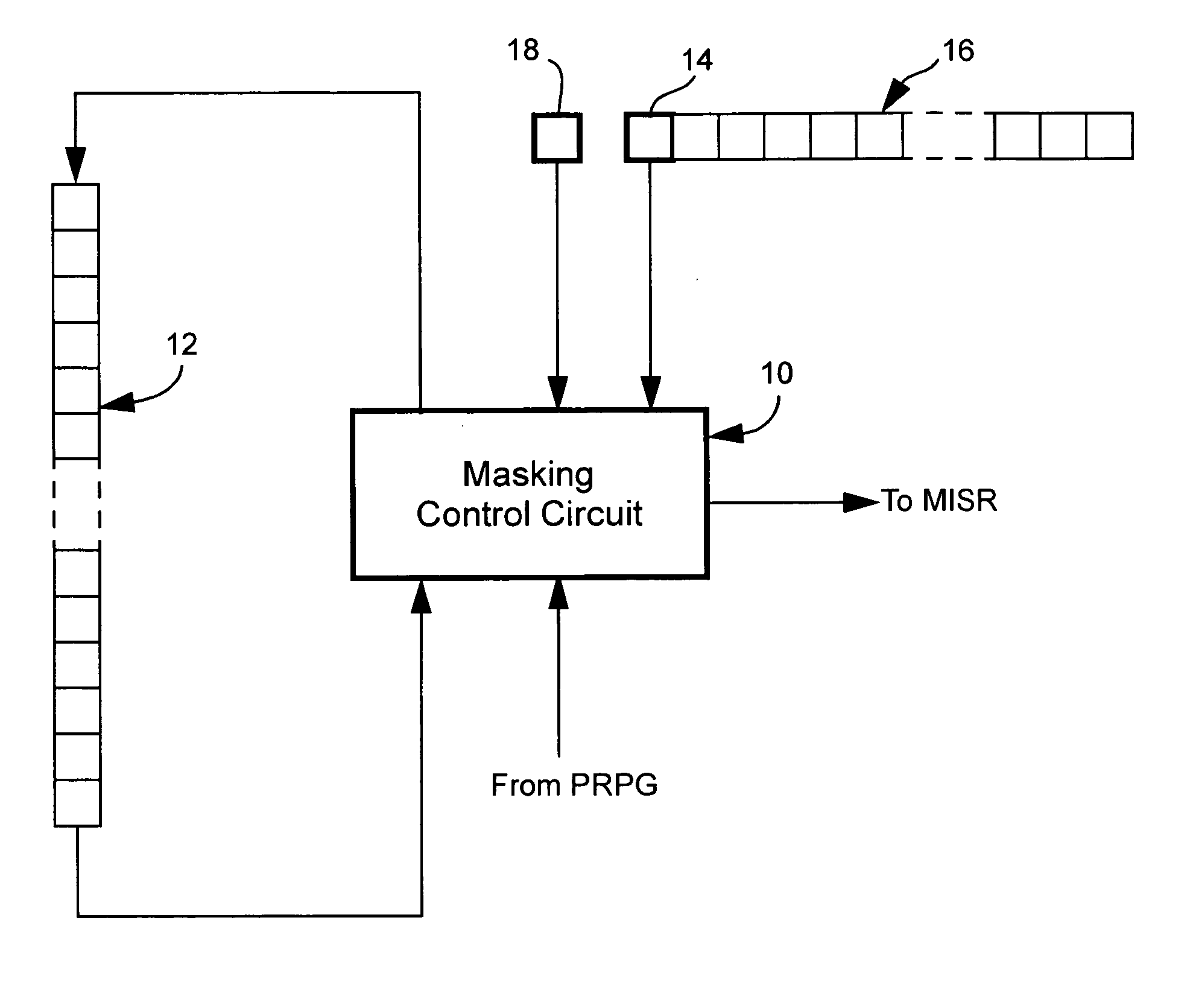
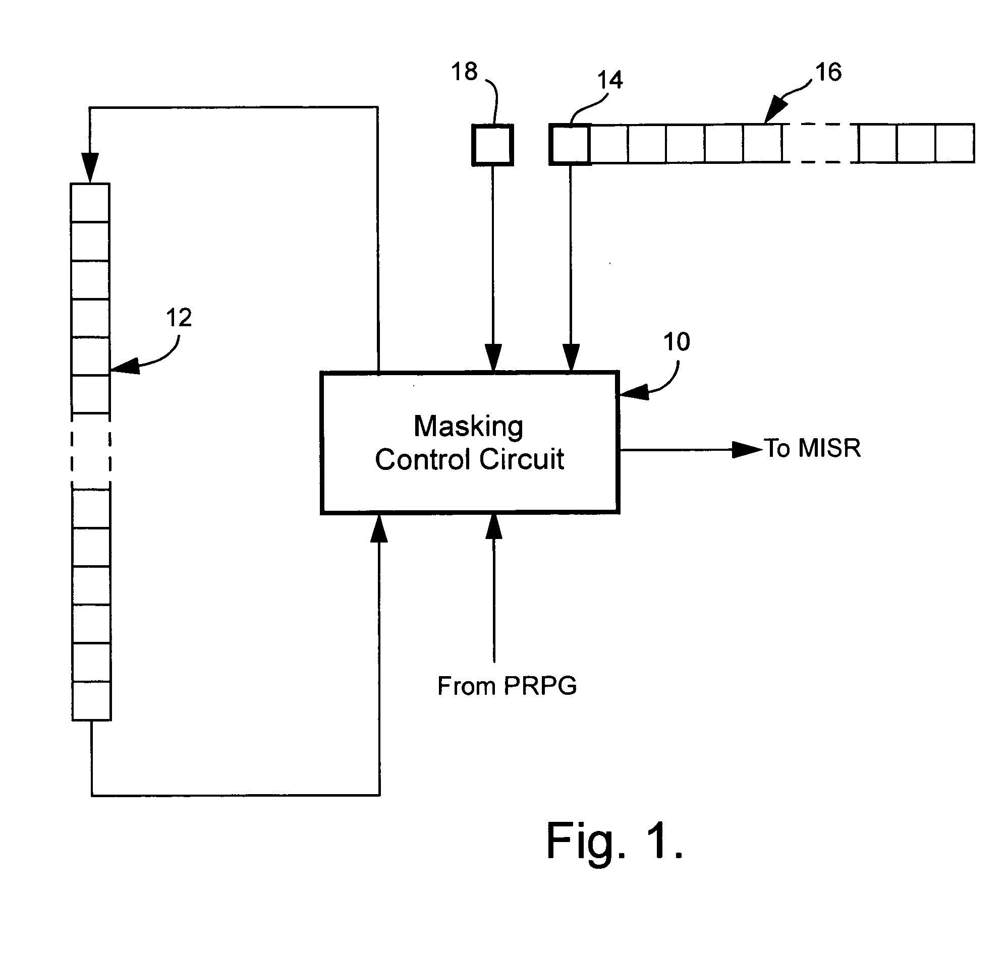
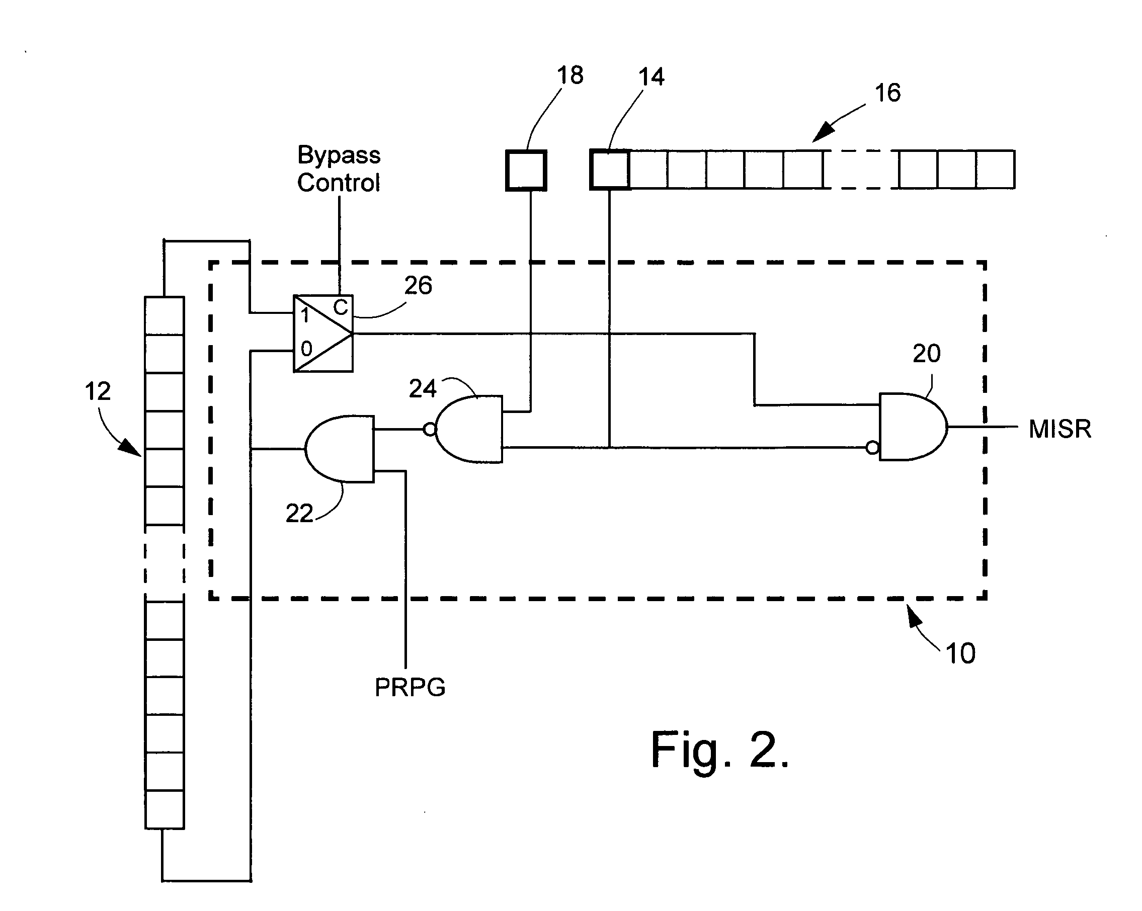
[0025] In general, the present invention provides a masking circuit for selectively masking scan chain outputs and inputs during scan testing of an integrated circuit. The masking circuit comprises a mask register having at least two mask register elements for each scan chain to provide a plurality of masking modes; and an input and output mask control circuit for each scan chain. Each of the mask control circuits is connected between a test pattern source and a signature register and between a serial input and a serial output of an a...


PUM


Abstract

A masking circuit for selectively masking scan chain inputs and/or outputs during scan testing of an integrated circuit, comprises a mask register having at least two mask register elements for each scan chain to provide a plurality of masking modes; and an input and output mask control circuit for each scan chain, each mask control circuit being connected between a test pattern source and a signature register and between a serial input and a serial output of an associated scan chain and being responsive to mask control data stored in the register elements for configuring the associated scan chain in one of the plurality of masking modes during a scan test of the circuit.

Description

CROSS-REFERENCE TO RELATED APPLICATIONS [0001] This application claims the benefit of U.S. Provisional Patent Application Ser. No. 60 / 564,211 filed Apr. 22, 2004, incorporated herein by reference.BACKGROUND OF THE INVENTION [0002] 1. Technical Field [0003] The present invention generally relates to testing of integrated circuits and, more specifically, to a method of performing signature analysis in the presence of corrupted bits. [0004] 2. Description of Related Art [0005] Integrated circuits are now commonly designed with scan chains comprised of a plurality of scannable memory elements or scan cells. Each scan chain has a serial input for serially loading a test pattern into the scan chain and a serial output connected to a signature register through a masking circuit, described later. Memory elements which form the scan chains are connected to combinational logic circuits. During a scan test of a circuit, test patterns are loaded into the memory elements by shifting them through...

Claims


Application Information

Patent Timeline
Patent Type & Authority Applications(United States)
IPC IPC(8): G01R31/28G01R31/3185
CPCG01R31/318572
Inventor COTE, JEAN-FRANCOISPRICE, PAULNADEAU-DOSTIE, BENOIT
Owner LOGICVISION
Why Eureka
Try Eureka