Transimpedance Amplifier (TIA) Having an Enlarged Dynamic Range and Optical Devices Using the Same

Active Publication Date: 2016-09-15
SOURCE PHOTONICS CHENGDU
View PDF9 Cites 15 Cited by
  • Summary
  • Abstract
  • Description
  • Claims
  • Application Information

AI Technical Summary

Benefits of technology

[0013]Relative to prior approaches, the present invention provides the following advantages: when the optical input power is at a high level, the gain of the TIA can be reduced by adjusting the resistance value of the impedor such that the distortion of the TIA from overload can be improved; when the optical

Problems solved by technology

If the gain of the TIA is too great, the sensitivity requirement for low power optical input signals can be met, but the TIA will be fully overloaded or saturated if optical input power is above a certain power.
On t

Method used


Image

  • Transimpedance Amplifier (TIA) Having an Enlarged Dynamic Range and Optical Devices Using the Same
  • Transimpedance Amplifier (TIA) Having an Enlarged Dynamic Range and Optical Devices Using the Same
  • Transimpedance Amplifier (TIA) Having an Enlarged Dynamic Range and Optical Devices Using the Same

Examples


Example

A First Embodiment

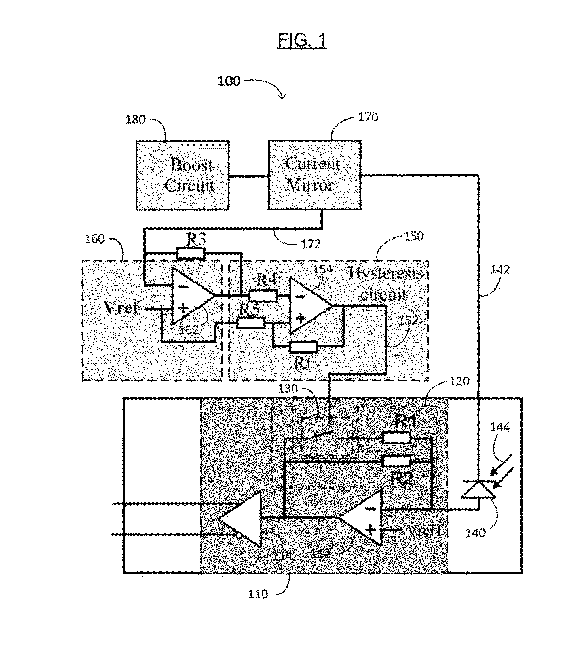
[0024]As shown in FIG. 1, an optical receiver 100 includes a TIA 110 having an improved dynamic range may include a current amplifier 112, an impedor 120, and a switch 130. The TIA 110 may further comprise a buffer 114 receiving an output of the current amplifier 112. In one embodiment, the buffer 114 is or comprises a differential output buffer (e.g., as shown), but which may also be or comprise a conventional single-ended buffer (i.e., providing a single-ended output signal, as opposed to a differential output signal). The TIA 100 is particularly useful in optical or optoelectronic devices, such as optical receivers and optical transmitters.

[0025]The current amplifier 112 has a reference voltage input terminal, a second input terminal, and an output terminal. The current amplifier 112 is configured to produce an amplified current (e.g., at the output terminal) from a received bias current. In one example, the bias current is provided by a photodiode 140, which co...

Example

A Second Embodiment

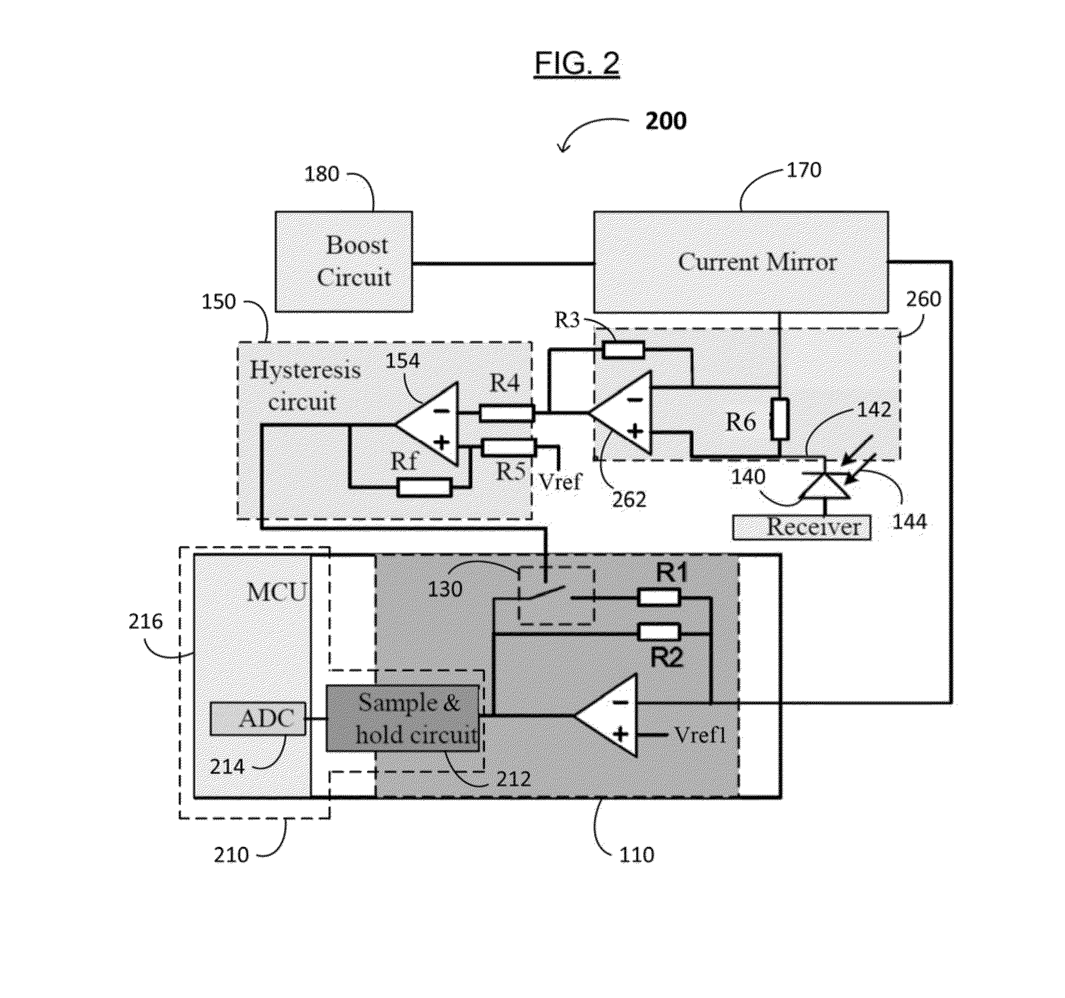
[0035]FIG. 2 shows an optical receiver 200, comprising a RSSI circuit 210 and the TIA 110 of FIG. 1. The optical receiver 200 may further include the hysteresis circuit 150. Since optical signals from other optical transmitters in the network may have any of a wide range of signal strengths (e.g., from −6 dBm to −34 dBm, from −8 dBm to −22 dBM, etc.), the RSSI circuit 210 should advantageously have good sensitivity over a wide range of signal strengths. When the optical input power is less than a medium threshold (such as −18 dBm), the amplifier should have a high gain (in which case the switch 130 may be off). Such a configuration is very helpful for ADC sampling, and provides improved accuracy (e.g., which is useful for an RSSI monitor). However, when the optical input power is higher than the medium threshold, especially in an overload range or section (such as at or near −6 dBm), the amplifier (e.g., amplifier 112 in FIG. 1) is saturated, so it is difficult fo...


PUM


Abstract

A gain-variable trans-impedance amplifier (TIA) in optical device is disclosed. The TIA has an improved dynamic range for receiving electrical signals and is configured to convert current signals from an avalanche photodiode (APD) to voltage signals. A resistor element is between the input and output terminals of the TIA, wherein the resistance of the resistor element can regulate the resistance and/or impedance value of the TIA, and a switch determines or controls the resistance of the resistor element. When the power of an optical signal received by the APD is higher than a predetermined value, the resistance becomes smaller and the gain of the TIA becomes greater. When the power of the optical signal is lower than the predetermined value, the resistance becomes greater. The gain of the TIA is automatically adjusted on the basis of the intensity of received optical signals to obtain a greater dynamic operational range.

Description

FIELD OF THE INVENTION[0001]The present invention relates to the field of optical communication devices. More specifically, embodiments of the present invention pertain to circuits configured to enlarge the dynamic range of trans-impedance amplifiers (TIAs) in optical devices.DISCUSSION OF THE BACKGROUND[0002]Optical transceivers send and receive optical data over an optical link, such as a fiber-optic link. An optical transmitter can include laser driver circuitry to drive a laser diode, such as a light-emitting diode (LED), to create optical pulses or signals on the fiber-optic link from received electronic signals. An optical receiver can include a photodiode to receive the optical signals, which are then converted into electronic signals. Thus, an optical transceiver converts (i) optical signals into analog and / or digital electronic signals and (ii) electronic signals into optical signals.[0003]The receiver (RX) of an optical transceiver generally comprises at least one photodio...

Claims


Application Information

Patent Timeline
IPC IPC(8): H03F3/08H04B10/25H04B10/69H03K3/037
CPCH03F3/08H04B10/69H04B10/25H03K3/0377H03F3/087H03F1/083H03F3/45475H03F2203/45522H03F2203/45528H03F2203/45536H03G3/3084H04B10/6931
Inventor JIANG, XUSONG, YUANZHANG, SHUYUANXU, YUANZHONG
Owner SOURCE PHOTONICS CHENGDU
Why Eureka
Try Eureka