Method and arrangement for layout and manufacture of nonmanhattan semiconductor integrated circuit using simulated euclidean wiring

a technology of simulated euclidean wiring and semiconductor integrated circuit, which is applied in the direction of computer aided design, semiconductor/solid-state device details, instruments, etc., can solve the problems of designers having to return to earlier steps and the task of routing a typical integrated circuit is a very difficult task

Inactive Publication Date: 2005-10-27
CADENCE DESIGN SYST INC
View PDF9 Cites 39 Cited by
  • Summary
  • Abstract
  • Description
  • Claims
  • Application Information

AI Technical Summary

Problems solved by technology

Generally, detailed routing systems use a routing grid that specifies a very limited set of possible locations for the various electrical interconnect signals.
Note that problems may occur during various steps of the integrated circuit layout forcing the designers to return to earlier steps.
The task of routing a typical integrated circuit is a very difficult task due to the large number of interconnect lines that must be routed and the extremely large number of possible different routing paths.

Method used


Image

  • Method and arrangement for layout and manufacture of nonmanhattan semiconductor integrated circuit using simulated euclidean wiring
  • Method and arrangement for layout and manufacture of nonmanhattan semiconductor integrated circuit using simulated euclidean wiring
  • Method and arrangement for layout and manufacture of nonmanhattan semiconductor integrated circuit using simulated euclidean wiring

Examples


Embodiment Construction

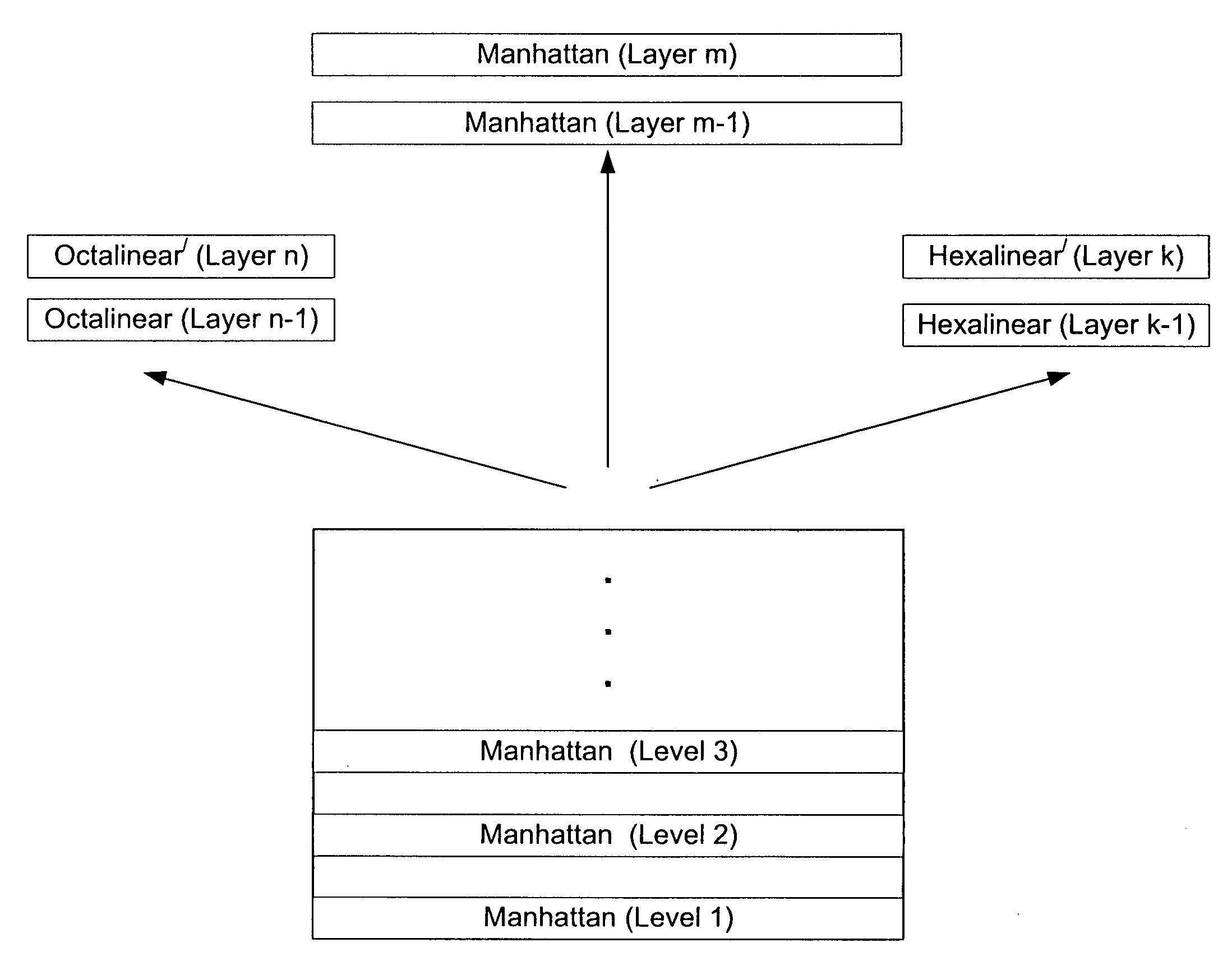
[0067] Gridless non Manhattan integrated circuit (“IC”) architectures and methods for designing and manufacturing gridless non Manhattan integrated circuits are disclosed. In the following description, for purposes of explanation, specific nomenclature is set forth to provide a thorough understanding of the present invention. However, it will be apparent to one skilled in the art that these specific details are not required in order to practice the present invention. For example, the present invention has mainly been described with reference to a non Manhattan routing system that uses two layers of orthogonal 45° angle wiring and a non Manhattan routing system that uses plus 60° angle wiring and negative 60° wiring. However, the same techniques can easily be applied to many other types of gridless non Manhattan routing systems.

Routing Architectures

[0068] Most existing semiconductors use the “Manhattan” wiring model that specifies alternating layers of preferred-direction horizonta...


PUM


Abstract

Some embodiments provide an integrated circuit that includes several circuits. The integrated circuit further includes a first interconnect wiring layer that has a first preferred direction of interconnect wiring. The integrated circuit also includes a second interconnect wiring layer that has a second preferred direction of interconnect wiring, where the first and second preferred directions of interconnect wiring are neither orthogonal nor parallel. The integrated circuit also includes several interconnect wiring on the first and second interconnect wiring layers that couples the circuits and are not aligned with any grid other than a manufacturing grid.

Description

FIELD OF THE INVENTION [0001] The present invention relates to the field of semiconductor design and manufacture. In particular the present invention discloses gridless semiconductor architectures and methods for designing and manufacturing gridless semiconductor integrated circuits. BACKGROUND OF THE INVENTION [0002] An integrated circuit (“IC”) is a semiconductor device that includes many electronic components (e.g., transistors, diodes, inverters, etc.). These electrical components are interconnected to form larger scale circuit components (e.g., gates, cells, memory units, arithmetic units, controllers, decoders, etc.) on the IC. The electronic and circuit components of IC's are jointly referred to below as “components.”[0003] An IC also includes multiple layers of metal and / or polysilicon wiring that interconnect its electronic and circuit components. For instance, many IC's are currently fabricated with five metal layers. In theory, the wiring on the metal layers can be all-an...

Claims


Application Information

Patent Timeline
Patent Type & Authority Applications(United States)
IPC IPC(8): G06F17/50
CPCG06F17/5077G06F30/394
Inventor TEIG, STEVENCALDWELL, ANDREW
Owner CADENCE DESIGN SYST INC
Why Eureka
Try Eureka