Method for manufacturing grid line with high uniformity through double exposure

A gate line, double exposure technology, applied in microlithography exposure equipment, photolithography process exposure equipment, semiconductor/solid-state device manufacturing, etc., can solve the problems of limited uniformity, complex process, low production capacity, etc. cost, simplify the production process, and improve the effect of production capacity

Active Publication Date: 2014-01-01
SHANGHAI HUALI MICROELECTRONICS CORP
View PDF4 Cites 5 Cited by
  • Summary
  • Abstract
  • Description
  • Claims
  • Application Information

AI Technical Summary

Problems solved by technology

However, the process of the above scheme is relatively complicated, the ...

Method used


Image

  • Method for manufacturing grid line with high uniformity through double exposure
  • Method for manufacturing grid line with high uniformity through double exposure
  • Method for manufacturing grid line with high uniformity through double exposure

Examples


no. 1 example

[0049] Figure 4A to Figure 4G It schematically shows a method for manufacturing gate lines with high uniformity by double exposure according to the first preferred embodiment of the present invention.

[0050] Specifically, as Figure 4A to Figure 4G As shown, the method for making gate lines with high uniformity by double exposure according to a preferred embodiment of the present invention includes:

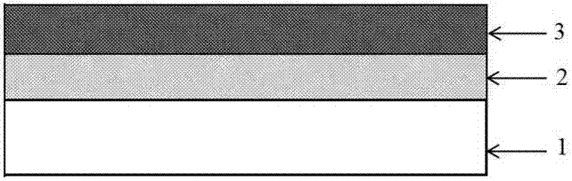
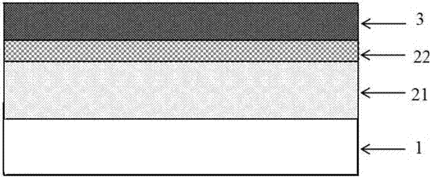
[0051] The first step: deposit polysilicon film 4, amorphous carbon film 21, and carbon-containing silicon oxide film 22 successively on substrate silicon wafer 1, and then coat the first photoresist 3 of formable hard film, such as Figure 4A shown;

[0052] The second step: finish exposing and developing so as to form the structure of the first gate lines 31 in the first photoresist 3 film, such as Figure 4B shown;

[0053] The third step: in the same development machine as the development of the second step, the silicon wafer with the first gate line 31 structure in th...

no. 2 example

[0059] Figure 4A to Figure 4G It schematically shows a method for fabricating gate lines with high uniformity by double exposure according to the second preferred embodiment of the present invention.

[0060] Specifically, as Figure 4A to Figure 4G As shown, the method for making gate lines with high uniformity by double exposure according to a preferred embodiment of the present invention includes:

[0061] The first step: deposit polysilicon film 4, amorphous carbon film 21, and carbon-containing silicon oxide film 22 successively on substrate silicon wafer 1, and then coat the first photoresist 3 of formable hard film, such as Figure 4A shown;

[0062] The second step: finish exposing and developing so as to form the structure of the first gate lines 31 in the first photoresist 3 film, such as Figure 4B shown;

[0063] The third step: in the same development machine as the development of the second step, apply a silylation material liquid on the first photoresist 3 ...

Embodiment approach

[0069] Preferably, the first photoresist 3 capable of forming the hard film is a photoresist containing one or more of silyl, siloxyl and silsesquioxane.

[0070] Preferably, the etching resistance ratio of the first photoresist 3 and the second photoresist 5 is greater than or equal to 1.5:1.

[0071] Preferably, the silylating material is hexamethyldisilazine (HMDS, hexamethyldisilazine), trimethylchlorosilane (TMCS, trimethylchlorosilane), hexamethyldisilazane (HMDSZ, hexamethyldisilazane), or other applicable silylating materials one or more of.

[0072] Preferably, the heating temperature in the third step ranges from 80°C to 300°C. Further preferably, the heating temperature in the third step ranges from 90°C to 200°C.

[0073] Preferably, the thickness of the amorphous carbon thin film 21 is 20 nm to 300 nm. Further preferably, the thickness of the amorphous carbon film 21 is 50 nm to 250 nm.

[0074] Preferably, the carbon-containing silicon oxide film 22 has a thi...


PUM

PropertyMeasurementUnit
Thicknessaaaaaaaaaa
Thicknessaaaaaaaaaa
Thicknessaaaaaaaaaa

Abstract

The invention provides a method for manufacturing a grid line with high uniformity through double exposure. The method comprises the following steps: sequentially depositing a polycrystalline silicon thin film, an amorphous carbon thin film and a silicon oxide thin film containing carbon, and then coating, so as to form a first photoresist for a hard film; performing exposure and development to form a first grid line structure in a first photoresist film; curing the first grid line structure, and heating, so as to enable a silanization material to react with the surface of the first photoresist to form an isolating film which is insoluble in a second photoresist; coating the second photoresist on the cured first photoresist; performing exposure and development to form a first line end cutting figure in a second photoresist film; etching the isolating film and a first line by using the second photoresist film as a mask, so as to form a second line end cutting figure; sequentially etching all films by using the rest isolating film and the first grid line as the mask, and finally forming a second grid line structure in the polycrystalline silicon thin film.

Description

technical field [0001] The invention relates to the field of semiconductor manufacturing, and more specifically, the invention relates to a method for manufacturing high-uniformity gate lines by double exposure. Background technique [0002] As the integration level of semiconductor chips continues to increase, the feature size of transistors continues to shrink, posing more and more challenges to the photolithography process. The traditional photolithography process usually adopts organic bottom anti-reflective coating (BARC) with polymer materials as the main body to improve the capability of the photolithography process. Figure 1A It is a schematic diagram of the structure of the substrate silicon wafer 1, the organic anti-reflection film 2, and the photoresist 3. The organic anti-reflection film can also expand the adjustable range of the etching process and improve the uniformity of the pattern structure after etching. [0003] After entering the 45nm technology node,...

Claims


Application Information

Patent Timeline
IPC IPC(8): G03F7/20H01L21/027
Inventor 毛智彪
Owner SHANGHAI HUALI MICROELECTRONICS CORP
Why Eureka
Try Eureka