Monolithic integrated manufacturing method for indium phosphide-based resonant tunneling diodes and high-electron-mobility transistors

A technology with high electron mobility and manufacturing method, applied in semiconductor/solid-state device manufacturing, circuits, electrical components, etc., can solve problems affecting production and application, and achieve high yield, good practicability, and strong operability. Effect

Inactive Publication Date: 2010-04-07
NO 55 INST CHINA ELECTRONIC SCI & TECHNOLOGYGROUP CO LTD
View PDF0 Cites 5 Cited by
  • Summary
  • Abstract
  • Description
  • Claims
  • Application Information

AI Technical Summary

Problems solved by technology

[0007] The purpose of the present invention is to invent an indium phosphide-based Monolithic Integra

Method used


Image

  • Monolithic integrated manufacturing method for indium phosphide-based resonant tunneling diodes and high-electron-mobility transistors
  • Monolithic integrated manufacturing method for indium phosphide-based resonant tunneling diodes and high-electron-mobility transistors

Examples


Embodiment Construction

[0033] The present invention will be further described below in conjunction with the accompanying drawings and embodiments.

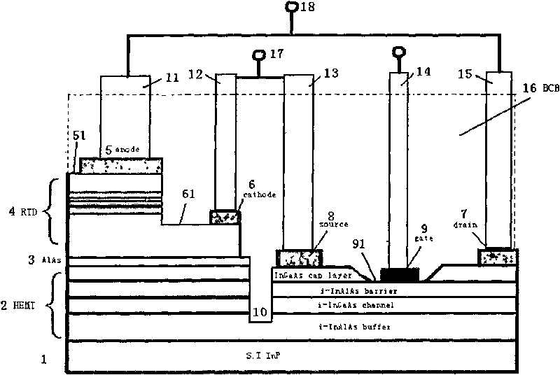
[0034] Such as figure 1 shown.

[0035] A method for monolithically integrating an indium phosphide-based resonant tunneling diode and a high electron mobility transistor, comprising the following steps:

[0036] Step 1: On the semiconductor material indium phosphide (InP) substrate 1, use molecular beam epitaxy (MBE) equipment to grow high electron mobility transistor (HEMT) material layer 2, aluminum arsenic (AlAs) isolation self-stop layer 3 and resonance in sequence Tunneling diode (RTD) material layer 4 structure; wherein aluminum arsenic (AlAs) isolates the self-stop layer 3 to realize the corrosion self-stopping of succinic acid (SA) etching solution, and simultaneously realizes the resonant tunneling diode material 4 and high electron mobility transistor Isolation of material 2;

[0037] Step 2: On the resonant tunneling diode (RTD) material ...


PUM


Abstract

The invention provides a monolithic integrated manufacturing method for indium phosphide-based resonant tunneling diodes and high-electron-mobility transistors, which comprises the following basic steps: orderly growing high-electron-mobility transistor and resonant tunneling diode materials on a semiconductor material indium phosphide (InP) substrate with molecular beam epitaxial equipment; etching the surface of an epitaxial wafer with electron beams, and forming the mesa of the resonant tunneling diodes through optical lithography and wet etching; realizing the isolation between devices through the optical lithography and the wet etching to form isolated channels; manufacturing upper and lower electrodes of the resonant tunneling diodes and source electrodes and drain electrodes of the high-electron-mobility transistors through metal ohmic contact, and then annealing; manufacturing grid electrodes through electron beam lithography, dry etching and wet etching; manufacturing metal terminals through dry etching, optical lithography and electron beam evaporation; and finally, interconnecting the resonant tunneling diodes and the high-electron-mobility transistors through a benzocyclobutene flatness process and metal wiring. The method has the characteristics of simple process, strong operability, high finished product ratio and the like, and has good practicability.

Description

technical field [0001] The invention relates to a method for manufacturing a transistor, in particular to an integrated method for manufacturing a resonant tunneling diode and a high electron mobility transistor, in particular to a method for realizing phosphorization by benzocyclobutene (BCB) planarization technology A method for monolithically integrating an indium-based resonant tunneling diode (RTD) and a high electron mobility transistor (HEMT). Background technique [0002] After nearly 20 years of research, it shows that InP materials are one of the electronic materials with the best performance so far. etc. have obvious advantages, and will be the mainstream material for the development of high-speed devices in the future. [0003] Resonant tunneling diode (RTD) is a negative resistance nanoelectronic device based on the quantum tunneling effect. It has the characteristics of fast response, high operating frequency, and low power consumption. The RTD can be connecte...

Claims


Application Information

Patent Timeline
IPC IPC(8): H01L21/77H01L21/329H01L21/335
Inventor 韩春林邹鹏辉陈辰程伟
Owner NO 55 INST CHINA ELECTRONIC SCI & TECHNOLOGYGROUP CO LTD
Why Eureka
Try Eureka