
Eureka
For R&D, Eureka makes reading and utilizing patents & technical documents easy.
Eureka AIR
Designed for self-driven R&D workflows. Generate viable solutions, solve complex R&D challenges, empower your innovation with AI.

Eureka Materials
Designed for material experts only. Revolutionize your material R&D, from search, analyze, to developing new materials.

TechResearch
Generate reliable direction feasibility study reports for your R&D in just a few steps.

TechSeek
Discover and master advanced knowledge NOW. Basics, ideas, possibilities, all at once.

TechMind
As an expert in R&D Theories, TechMind can generates customized viable solutions instantly.

TechRisk
Analyze your overall solution with one click, know your potential R&D risks in advance.

TechMonitor
Get weekly tech updates, stay abreast of the latest tech innovations and key insights.
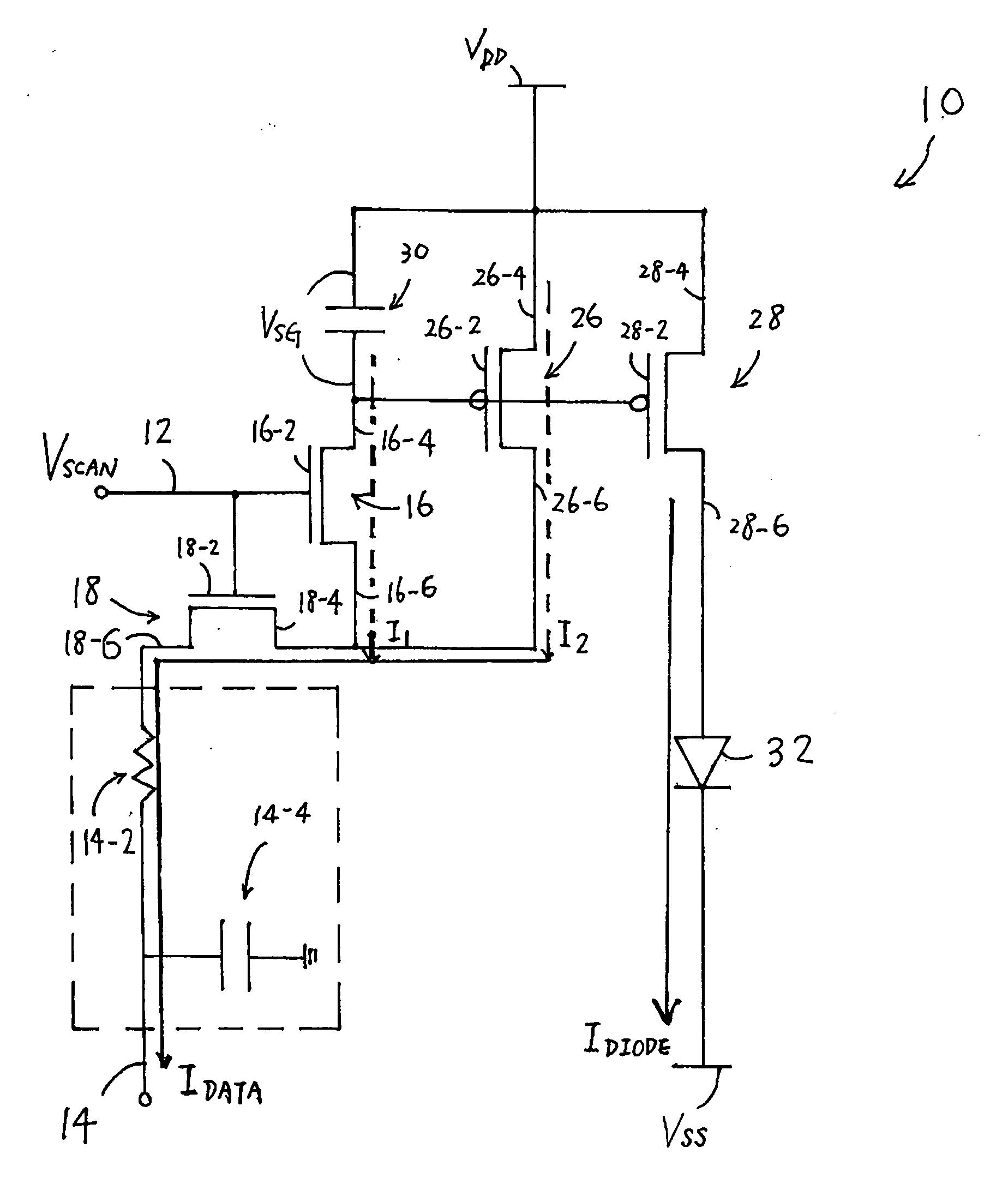
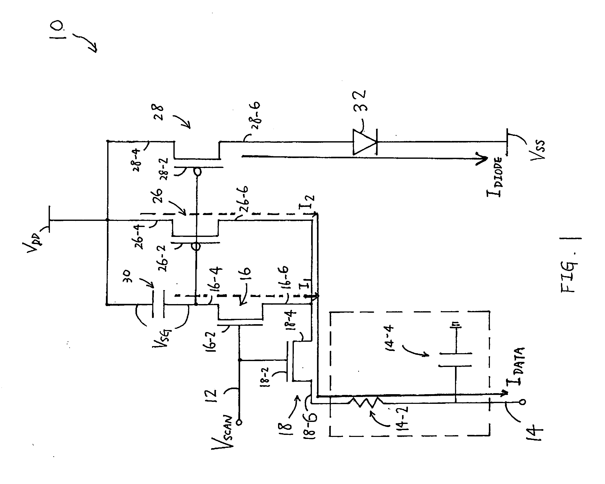
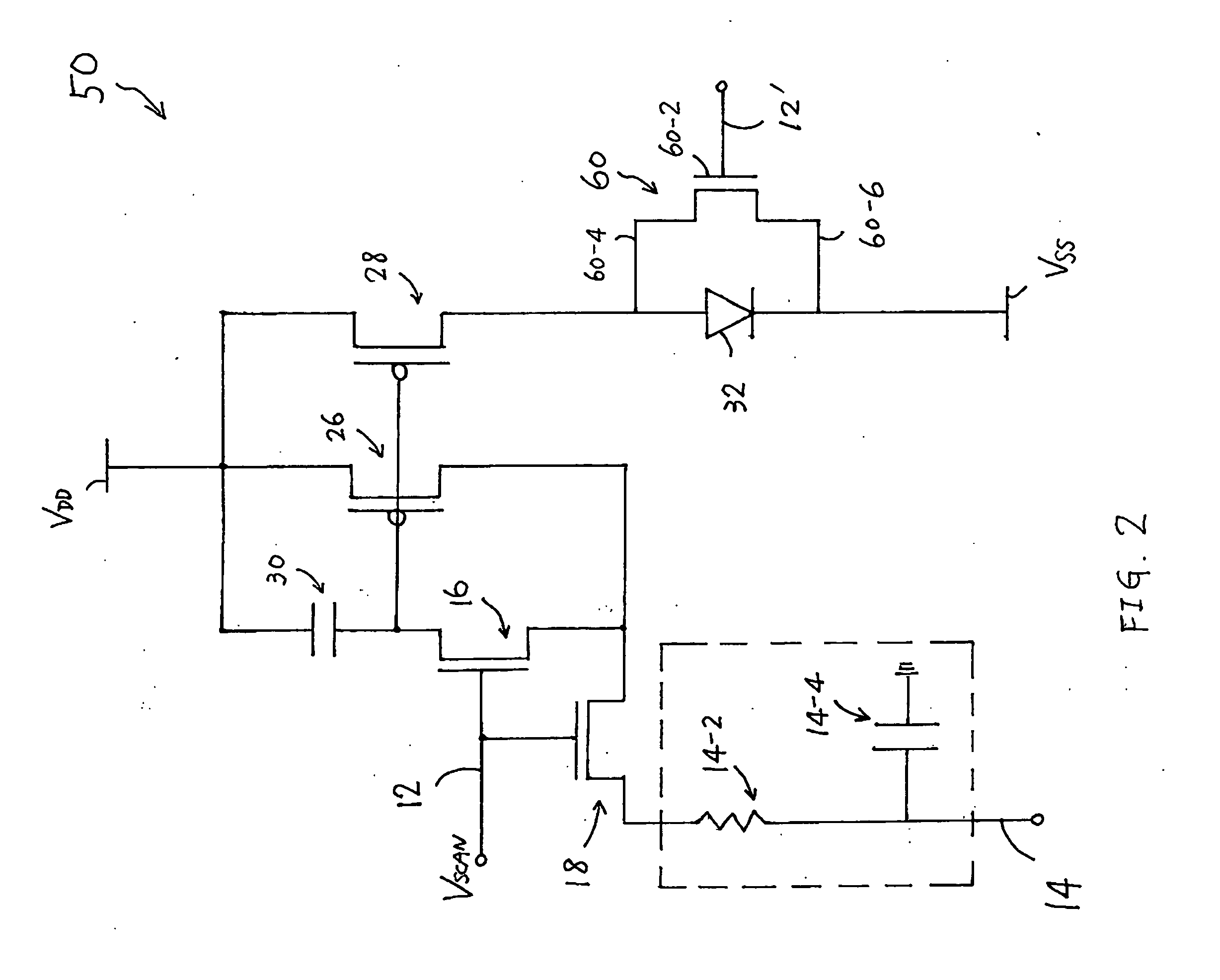
Current-driven OLED pixel
- Summary
- Abstract
- Description
- Claims
- Application Information
AI Technical Summary
Benefits of technology
Problems solved by technology
Method used
Image

Examples
Embodiment Construction
[0001] 1. Field of the Invention
[0002] This invention relates in general to an electroluminescence device and, more particularly, to a pixel element of an organic electroluminescence device.
[0003] 2. Background of the Invention
[0004] An electroluminescence (“EL”) device is a device which makes use of the phenomenon of electro luminescence to emit light. An EL device generally includes thin film transistors (“TFT”) and a light-emitting diode (“LED”) further including a light-emitting layer. If the light-emitting layer contains organic light-emitting material, the device is referred to as an organic EL device. When a current passes between a cathode and an anode of the LED device, light is emitted through the light-emitting layer.
[0005] Typically, EL devices may be classified into voltage-driven and current-driven types. As compared to a current-driven EL device, a voltage-driven EL device may be disadvantageous in non-uniform pixel brightness caused by different threshold voltage...
PUM
 Abstract
Description
Claims
Application Information
 - R&D Engineer
- R&D Manager
- IP Professional
- Industry Leading Data Capabilities
- Powerful AI technology
- Patent DNA Extraction
Browse by: Latest US Patents, China's latest patents, Technical Efficacy Thesaurus, Application Domain, Technology Topic, Popular Technical Reports.
© 2024 PatSnap. All rights reserved.Legal|Privacy policy|Modern Slavery Act Transparency Statement|Sitemap|About US| Contact US: help@patsnap.com