
Pin coupler for an integrated circuit tester

Active Publication Date: 2005-11-03
ADVANTEST CORP
View PDF5 Cites 17 Cited by
  • Summary
  • Abstract
  • Description
  • Claims
  • Application Information

AI Technical Summary

Benefits of technology

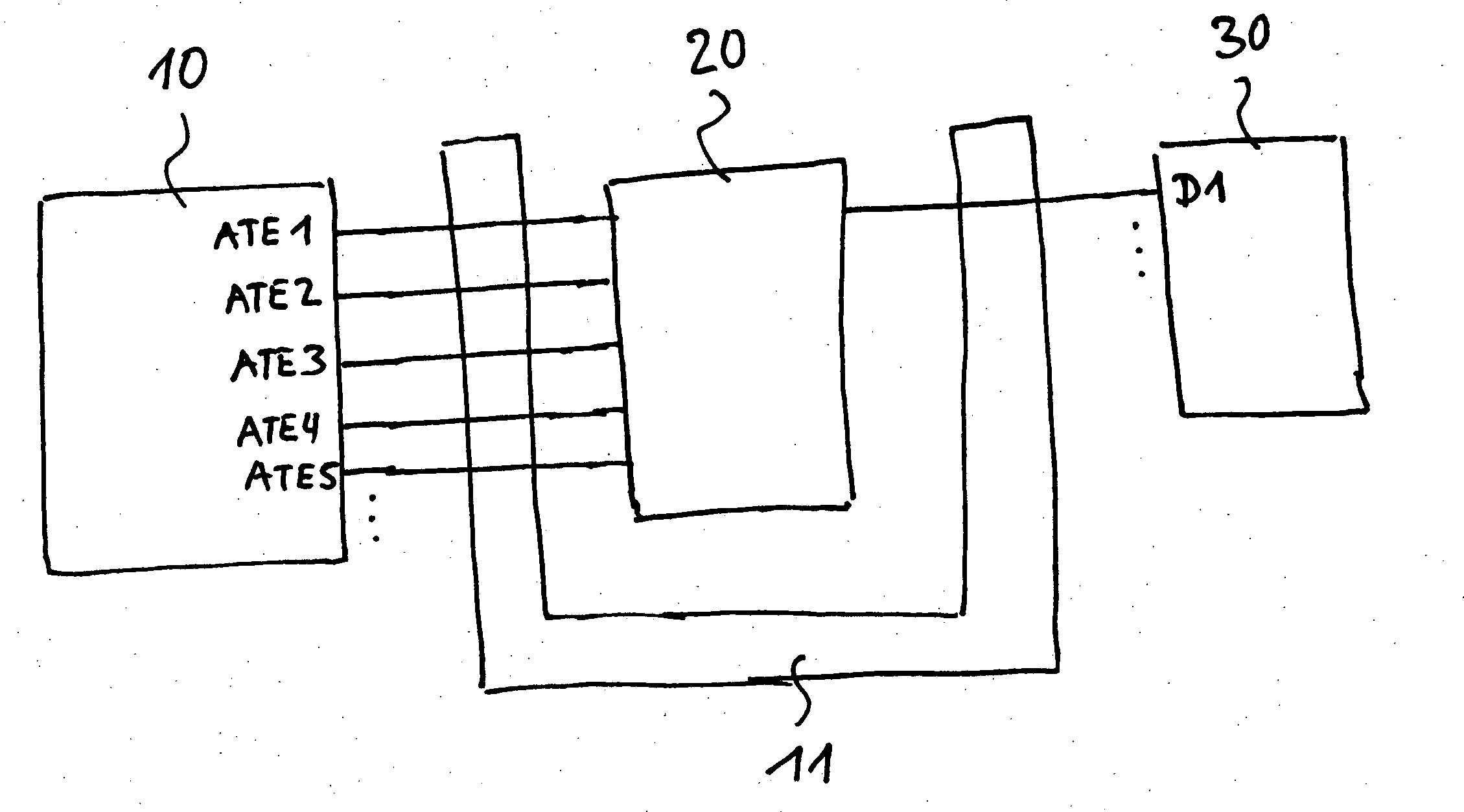
[0008] The invention thus allows for raising significantly the test data rate of existing testers without substantially changing the architecture or technology of the testers. Raising the test data rate can be simply achieved by additionally, providing a pin coupler for serializing and or parallelizing the test data and thus multiplying the data rate of existing testers.
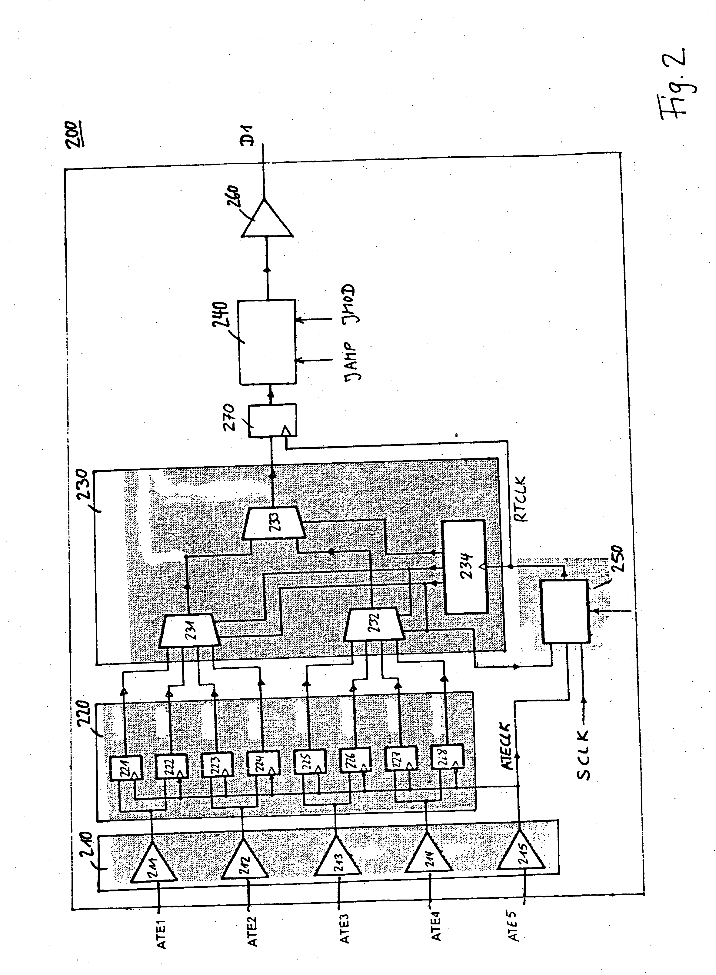
[0013] In yet a further embodiment of the invention, the synchronizing circuit comprises transfer elements or flip-flops for buffering, i.e. for short time storing and forwarding the data of the first stimulus data to a multiplexer circuit and wherein said transfer elements have trigger inputs for receiving the reference clock.
[0019] In a further embodiment, a plurality of the jitter insertion circuits are connected in series and each controlled by said first and second jitter modulation signal thus allowing for significantly increasing (i.e. multiplying) the jitter modulation depth.

Problems solved by technology

However, raising data rates of current ATEs is not possible without a fundamental architectural redesign.

Method used


Image

  • Pin coupler for an integrated circuit tester
  • Pin coupler for an integrated circuit tester
  • Pin coupler for an integrated circuit tester

Examples


first embodiment

[0034]FIG. 2 shows a channel coupler for serializing stimulus data received from ATE-pins, further referred to as channel serializer 200. ATE1-ATE4. Channel serializer 200 comprises an ATE Interface 210, a serializer synchronizing circuit 220, a multiplexing circuit 230, a high-speed transfer element or flip-flop 270, a serializer clock circuit 250, a jitter insertion circuit 240 and a DUT interface 260. ATE interface 210 comprises drivers 211-215 each connecting one ATE-pin ATE1-ATE4 to the data inputs of a pair of two single edge-triggered transfer elements or flip-flops 221-228 comprised by the serializer synchronizing circuit 220 and connecting the fifth ATE-pin ATE5 to the trigger inputs of the flip-flops 221-228, marked each by an arrow, and to clock circuit 250. The trigger inputs of the flip-flops from top to down are antivalent, being symbolized by a dot in front of every second trigger input. Clock circuit 250 receives a reference clock (signal) ATECLK from fifth ATE-pin A...

second embodiment

[0048]FIG. 3 shows a channel coupler adapted for working in the opposite direction compared to the channel serializer 200 shown in FIG. 2 and described above. The channel parallelizer 300 comprises a comparator 360, a high-speed flip-flop 350, a de-multiplexer circuit 340, a Parallelizer synchronizing circuit 320, an ATE-interface 310 and a parallelizer clock circuit 370. Comparator 360 is connected to the DUT-pin D1 receiving a high-speed response data signal from the DUT not shown in FIG. 3. ATE channels ATE1-ATE5 are again located on the left, whereas the DUT-pin is again located right. The signals flow is now mainly in the opposite direction, i.e. from the right side to left side. The signal flow is marked with arrows at the corresponding connections. However, similarly to FIG. 2, the fifth ATE channel ATE5 is again used for providing reference clock ATECLK to the channel coupler.

[0049] Comparator 360 receives at its inputs the high-speed data signal from DUT-pin D1 as well as a...


PUM


Abstract

A coupling unit that couples at least two pins of an ATE (Automated Test Equipment) to a pin of a device under test includes an ATE interface for receiving a plurality of first stimulus signals from selected ATE-pins and / or for sending a plurality of first response signals to the selected ATE-pins, a DUT interface for sending a second stimulus signal to the DUT-pin and / or for receiving a second response signal from the DUT-pin, and a multiplexer circuit for serializing data of the plurality of first stimulus signals into the second stimulus signal and / or a de-multiplexer circuit adapted for parallelizing data of the second response signal into the plurality of first response signals.

Description

BACKGROUND OF THE INVENTION [0001] The present invention relates to testing of integrated circuits with an automated test equipment. [0002] Integrated Circuits (IC) generally need to be tested to assure proper operation. This—in particular—is required during IC development and manufacturing. In the latter case, the ICs are usually tested before final application. During test, the IC, as a device under test (DUT), is exposed to various types of stimulus signals, and its responses are measured, processed and usually compared to an expected response of a good device. Automated test equipment (ATE) usually performs these tasks according to a device-specific test program. [0003] ATEs based various architectures have been applied for testing integrated circuits. For testing complex high speed circuits, ATEs with decentralized resources based on a per-pin architecture are known, wherein during test, each pin of a multiple of the pins of the DUT that are relevant for a test, is connected to...

Claims


Application Information

Patent Timeline
IPC IPC(8): G01R31/319G06F11/00G01R31/28
CPCG01R31/31905
Inventor ROTTACKER, MARKUSMOLL, JOACHIM
Owner ADVANTEST CORP
Learn More