

Overhang support for a stacked semiconductor device, and method of forming thereof
- Summary
- Abstract
- Description
- Claims
- Application Information
AI Technical Summary
Benefits of technology
Problems solved by technology
Method used
Image

Examples
Embodiment Construction
[0031] The making and using of the presently preferred embodiments are discussed below in detail. It should be appreciated, however, that the present invention provides many applicable inventive concepts that can be embodied in a wide variety of specific contexts. The specific embodiments discussed are merely illustrative of specific ways to make and use the invention, and do not limit the scope of the invention.
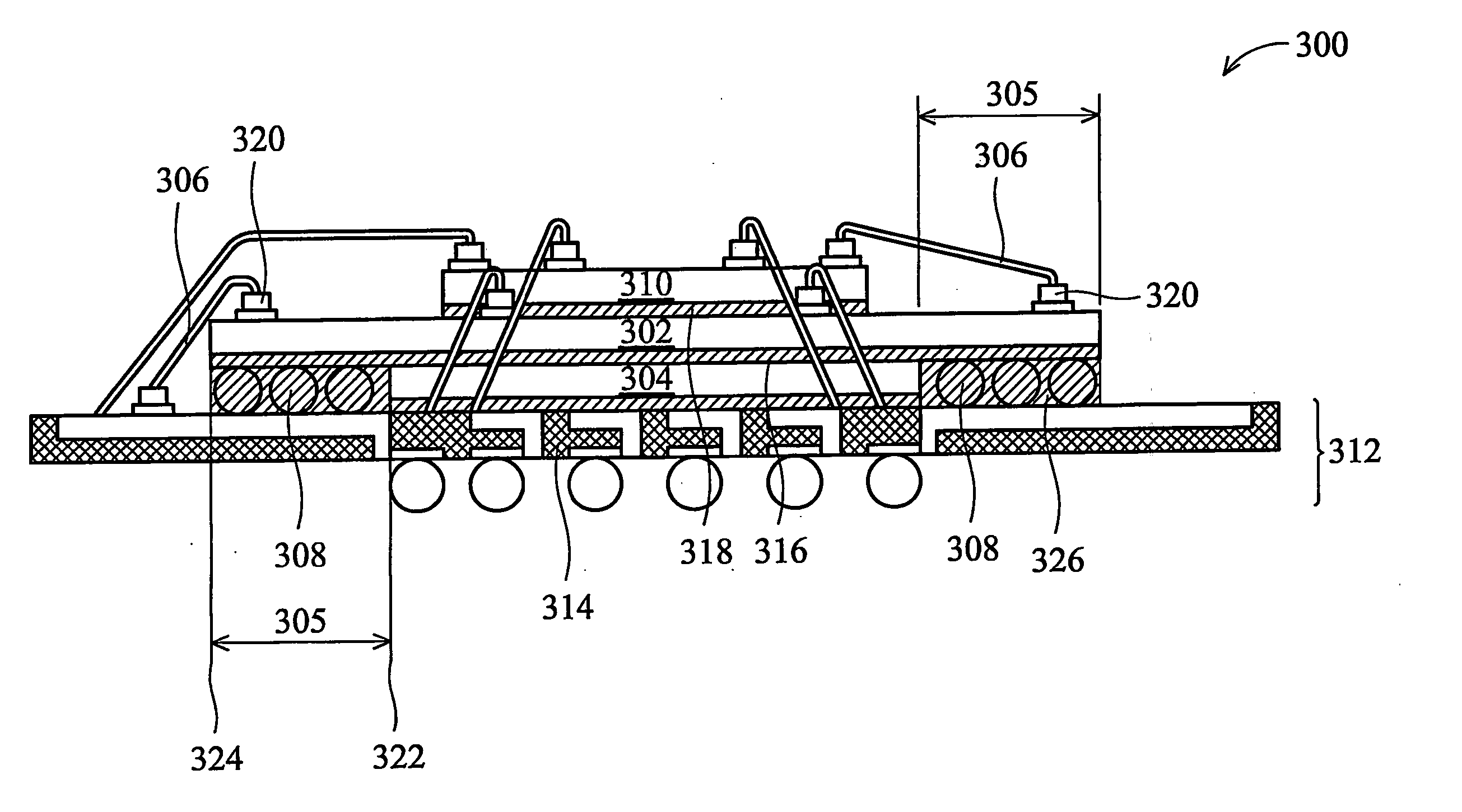
[0032] The present invention will be described with respect to preferred embodiments in a specific context, namely a semiconductor package comprising a substrate and two stacked dies. The invention may also apply, however, to other semiconductor devices that comprise more than two stacked dies, as well as to devices incorporating preferred embodiments of the invention on more than one level.
[0033] With reference now to FIG. 3, there is shown a cross sectional view of an upper die 182 and a lower die 180 stacked upon a substrate 184 in accordance with a preferred embodiment...
PUM
 Abstract
Description
Claims
Application Information