Optoelectronic module and method for producing an optoelectronic module

Active Publication Date: 2005-11-10
II VI DELAWARE INC
View PDF11 Cites 26 Cited by
  • Summary
  • Abstract
  • Description
  • Claims
  • Application Information

AI Technical Summary

Benefits of technology

[0030] This method makes it possible to produce the optoelectronic module at manufacturing sites for already known IC packages.
[0031] The carrier element is advantageously arranged in the opening of the leadframe. This makes it possible to form the carrier element as an exposed die.
[0032] In an advantageous development of the invention, wherein the leadframe is arranged on a film prior to the encapsulation with the plastic and said film is at least partly removed again after the encapsulation. This makes it possible for specific regions of the carrier element

Problems solved by technology

However, TO housings are relatively costly to

Method used


Image

  • Optoelectronic module and method for producing an optoelectronic module
  • Optoelectronic module and method for producing an optoelectronic module
  • Optoelectronic module and method for producing an optoelectronic module

Examples


Embodiment Construction

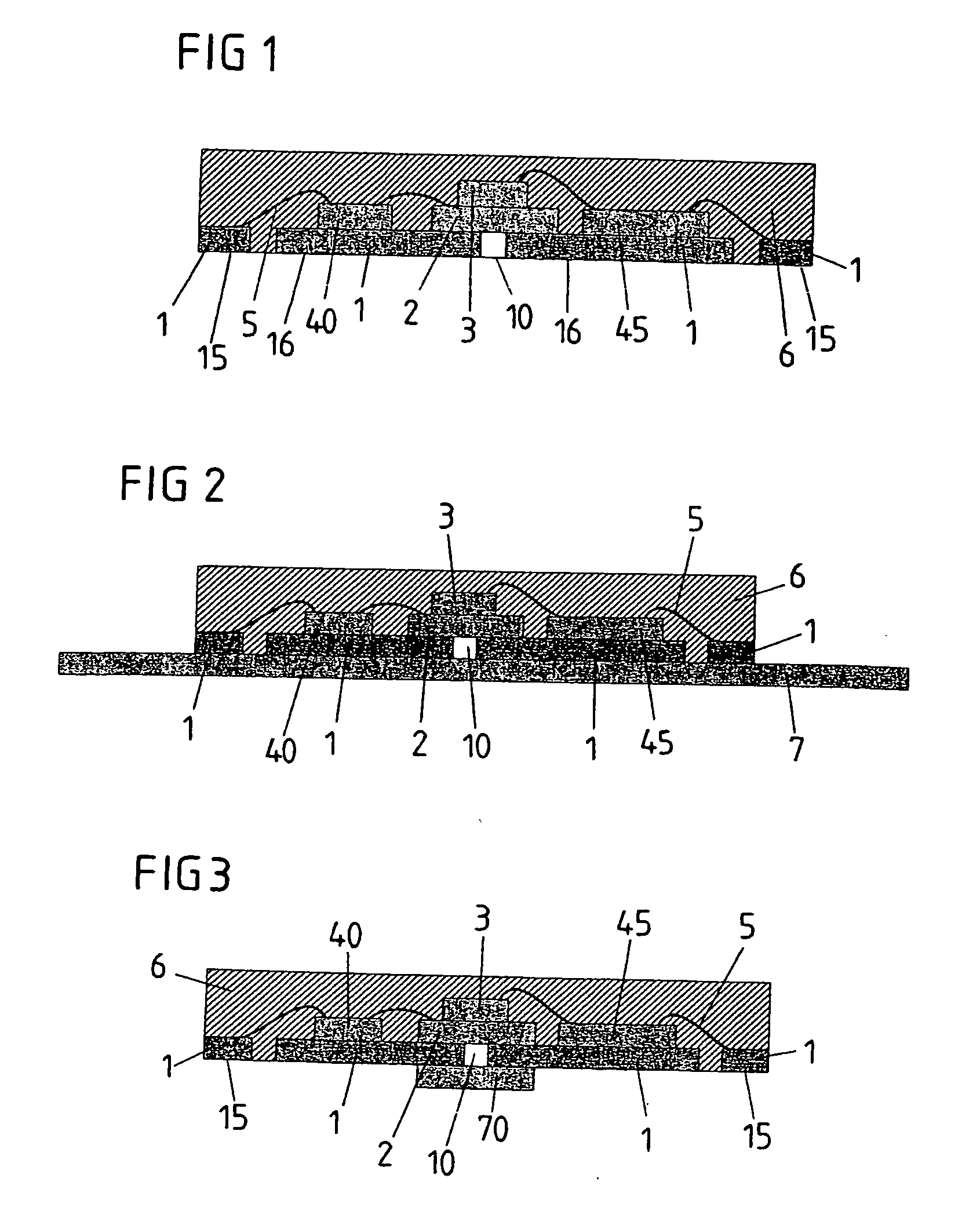
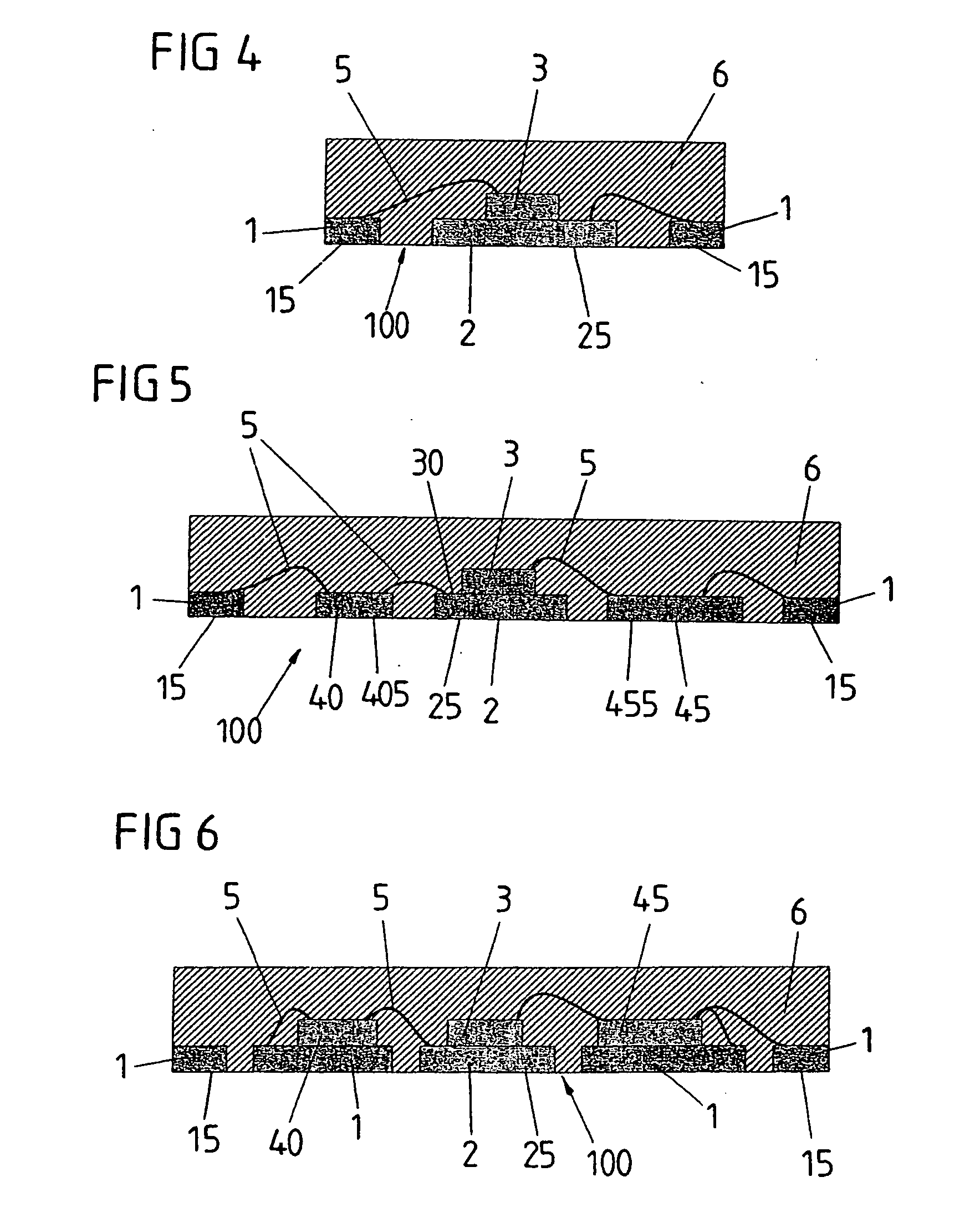
[0047] In the following detailed description of the figures, the same reference numerals are used for identical structural parts even though a plurality of different embodiments are involved.

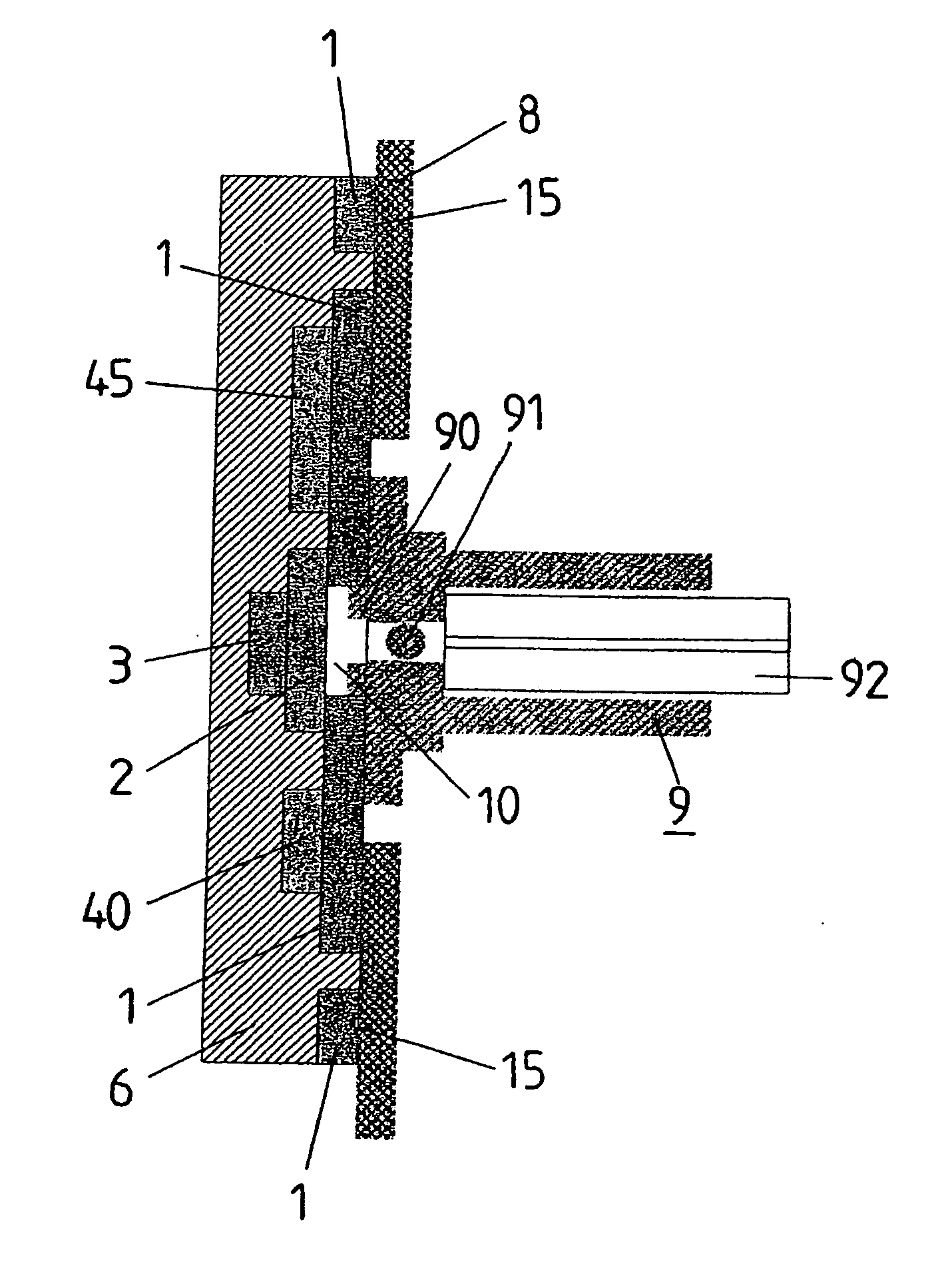
[0048]FIG. 1 shows a sectional illustration of an optoelectronic module. A leadframe 1 essentially forms the underside of the optoelectronic module. For this purpose, the leadframe 1 has contact areas 15 in the respective outer region of the optoelectronic module at the underside thereof, said contact areas being tin-coated. These tin-coated contact areas 15 serve for the mounting and electrical contact-connection of the optoelectronic module on a printed circuit board (not illustrated here). The optoelectronic module can thus be fitted on a printed circuit board for example by means of surface mounting.

[0049] The leadframe furthermore has surfaces 16 arranged in the inner region of the optoelectronic module on the underside thereof, which surfaces may likewise be connected to a printed circui...


PUM


Abstract

The invention relates to an optoelectronic module having at least one leadframe, at least one carrier element connected to the leadframe, and at least one optoelectronic component connected to the carrier element, which component can emit and/or receive light. The invention furthermore relates to a method for producing an optoelectronic module that includes providing at least one leadframe, at least one carrier element and at least one optoelectronic component, connecting the optoelectronic component to the carrier element and connecting the carrier element to the leadframe, and at least partly encapsulating the optoelectronic component, the carrier element and the leadframe with a plastic.

Description

[0001] The invention relates to an optoelectronic module in accordance with the preamble of claim 1 and to a method for producing an optoelectronic module in accordance with the preamble of claim 32. BACKGROUND OF THE INVENTION [0002] Optoelectronic components are becoming more and more important with regard to the rising requirements made of fast and reliable optical data transmission paths. In order to be able to efficiently fit the individual optoelectronic components into printed circuit board environments or printed circuit board layouts, they have to be processed to form corresponding modules or be incorporated into housings which have good radio frequency properties in order to enable high data rates. For this purpose, the optoelectronic components have hitherto been incorporated into TO housings having transparent windows. However, TO housings are relatively costly to manufacture and have a high structural height. [0003] DE 199 35 496 C1 discloses an optoelectronic component...

Claims


Application Information

Patent Timeline
IPC IPC(8): G02B6/12G02B6/26G02B6/42H01L27/146H01L31/0203H01L31/0232H01L33/48
CPCG02B6/4201G02B6/4204H01L2924/3025H01L2224/48247H01L2224/48137G02B6/4228H01L27/14618H01L27/14625H01L31/0203H01L31/0232H01L33/486H01L2224/48091H01L2924/00014H01L2924/00H01L2924/181G02B6/4283G02B6/4253G02B6/4255G02B6/4277G02B6/4281H01L31/02327H01L2924/00012
Inventor SCHRODINGER, KARL
Owner II VI DELAWARE INC
Why Eureka
Try Eureka