Method for manufacturing electro-optic device and electro-optic device

a manufacturing method and technology for optical devices, applied in non-linear optics, identification means, instruments, etc., can solve problems such as display defects, insufficient reduction of inter-substrat gap variations, and increase variations, so as to reduce the gap between substrates and reduce variations, the effect of increasing the height of the colored layer or the protective layer

Inactive Publication Date: 2005-11-17
SEIKO EPSON CORP
View PDF3 Cites 40 Cited by
  • Summary
  • Abstract
  • Description
  • Claims
  • Application Information

AI Technical Summary

Benefits of technology

[0010] An advantage of the invention is to provide a novel method for manufacturing an electro-optic device capable of decreasing variations in the gap between substrates, as compared with a conventional structure.
[0011] According to an aspect of the invention, a method for manufacturing an electro-optic device having a panel structure including an electro-optic material disposed between a pair of substrates, a spacer disposed between the pair of substrates to define the gap therebetween, and a color filter provided on one of the pair of substrates comprises a step of forming a substrate region to be used as the panel structure and a peripheral region to be separated from the substrate region on each of a pair of pre-substrates, a step of bonding the pair of sub-substrates together to form a pre-panel structure, and a step of dividing the pre-panel structure to form the panel structure, wherein a stacked structure including the spacer and a colored layer constituting the color filter or a protective film covering the color filter is disposed in the peripheral region of the pre-panel structure.
[0012] According to the aspect of the invention, the stacked structure including the spacer and the colored layer or the protective film is disposed in the peripheral region of the pre-panel structure, and thus the inter-substrate gap in the peripheral region can be securely defined by the stacked structure. In this case, the colored layer constituting the color filter and the protective film covering the color filter have a relatively large thickness, and the spacer is formed apart from the colored film and the protective film. Therefore, the inter-substrate gap in the peripheral region can be prevented from decreasing to be smaller than that in the portion to be used as the panel structure. Since the spacer is formed apart from the color filter, the spacer need not be formed in a stacked structure, and thus the height of the spacer can be precisely determined. Also, the colored layer or the protective layer overlapped with the spacer need not be formed in a restricted narrow region, and thus the precision of the height of the colored layer or the protective layer can be increased. Therefore, in bonding the pair of substrates together, the inter-substrate gap in the peripheral region can be precisely defined, and thus variations in the inter-substrate gap in the electro-optic device can be decreased as compared with a conventional structure.
[0013] According to another aspect of the invention, a method for manufacturing an electro-optic device having a panel structure including an electro-optic material disposed between a pair of substrates, a spacer disposed between the pair of substrates to define the gap therebetween, and a color filter provided on one of the pair of substrates comprises a step of forming a substrate region to be used as the panel structure and a peripheral region to be separated from the substrate region on each of a pair of pre-substrates, a step of bonding the pair of sub-substrates together to form a pre-panel structure, and a step of dividing the pre-panel structure to form the panel structure, wherein a stacked structure including the spacer and a colored layer constituting the color filter or a protective film covering the color filter is disposed within the substrate region and the peripheral region of the pre-panel structure.
[0014] The stacked structure preferably includes a laminate of a plurality of colored layers. When the stacked structure includes the laminate of a plurality of colored layers, the stacked structure can be formed to a large thickness. Therefore, even when a layered structure overlapped with the spacer in the panel structure is thick, the inter-substrate gap in the peripheral region can be made the same as that in the portion to be used as the panel structure.
[0015] The stacked structure preferably includes a laminate of the colored layer and the protective film. When the colored layer and the protective film are laminated, the stacked structure can be formed to a large thickness. Therefore, even when a layered structure overlapped with the spacer in the panel structure has a large thickness, the inter-substrate gap in the peripheral region can be made the same as that in the portion to be used as the panel structure.

Problems solved by technology

On the other hand, in a conventional electro-optic device, strong pressure is easily applied to the peripheries of substrates in a step of bonding the substrates together, and thus, in the periphery of a panel structure, the inter-substrate gap tends to decrease, thereby causing the problem of a display defect.
As a reaction, the inter-substrate gap at the edge of the portion to be used as each panel structure varies to cause the problem of increasing variations in the inter-substrate gap in the portion to be used as each panel structure.
There is thus the problem of failing to sufficiently decrease the variations in the inter-substrate gap in the peripheral portion of each panel structure.
However, the columnar spacer has an area greatly smaller than the pixel area, and thus, in some cases, a stacked structure comprising a plurality of colored layers cannot be wholly formed to a height enough to define the inter-substrate gap, and variations in the height of the spacer also increase.
Therefore, the spacer disclosed in the document has difficult in securing uniformity of the inter-substrate gap.
However, when the over-layer structure is used, the insulating film is laminated on the spacer in the panel structure, and, accordingly, the inter-substrate gap increases.

Method used


Image

  • Method for manufacturing electro-optic device and electro-optic device
  • Method for manufacturing electro-optic device and electro-optic device
  • Method for manufacturing electro-optic device and electro-optic device

Examples


Embodiment Construction

[0043] A method for manufacturing an electro-optic device and an electro-optic device according to an embodiment of the invention will be described in detail below with reference to the attached drawings.

Electro-Optic Device

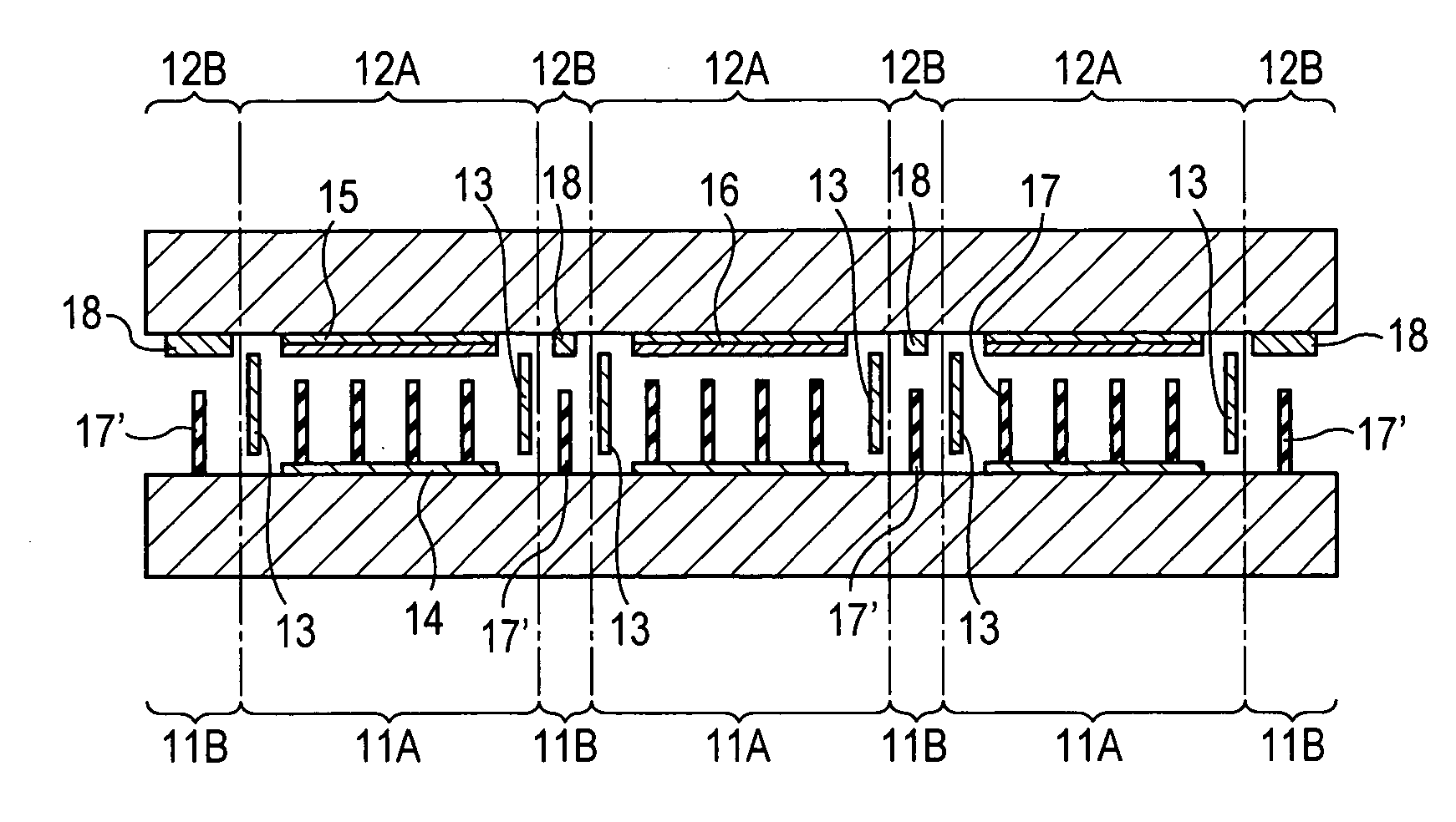
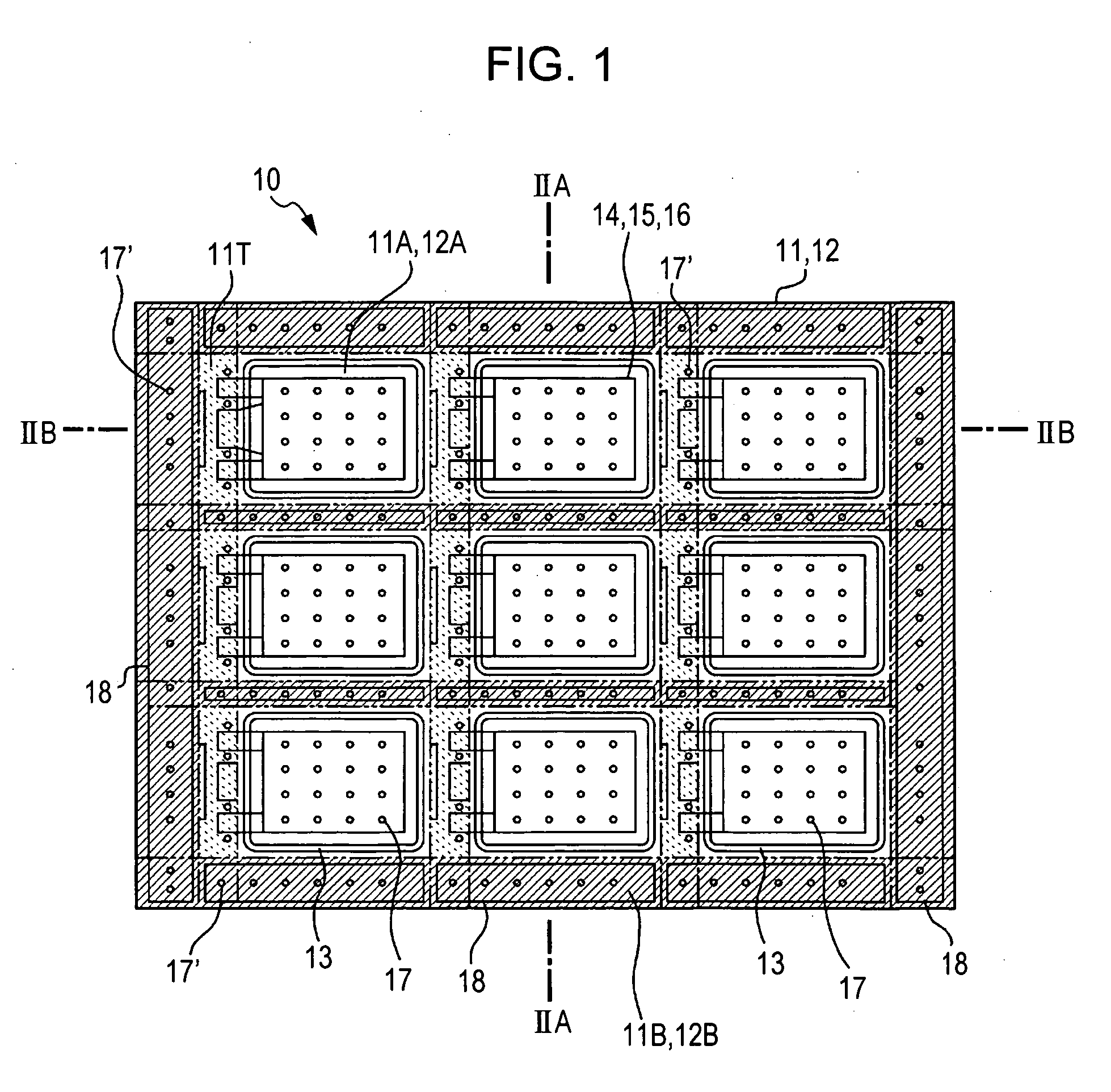
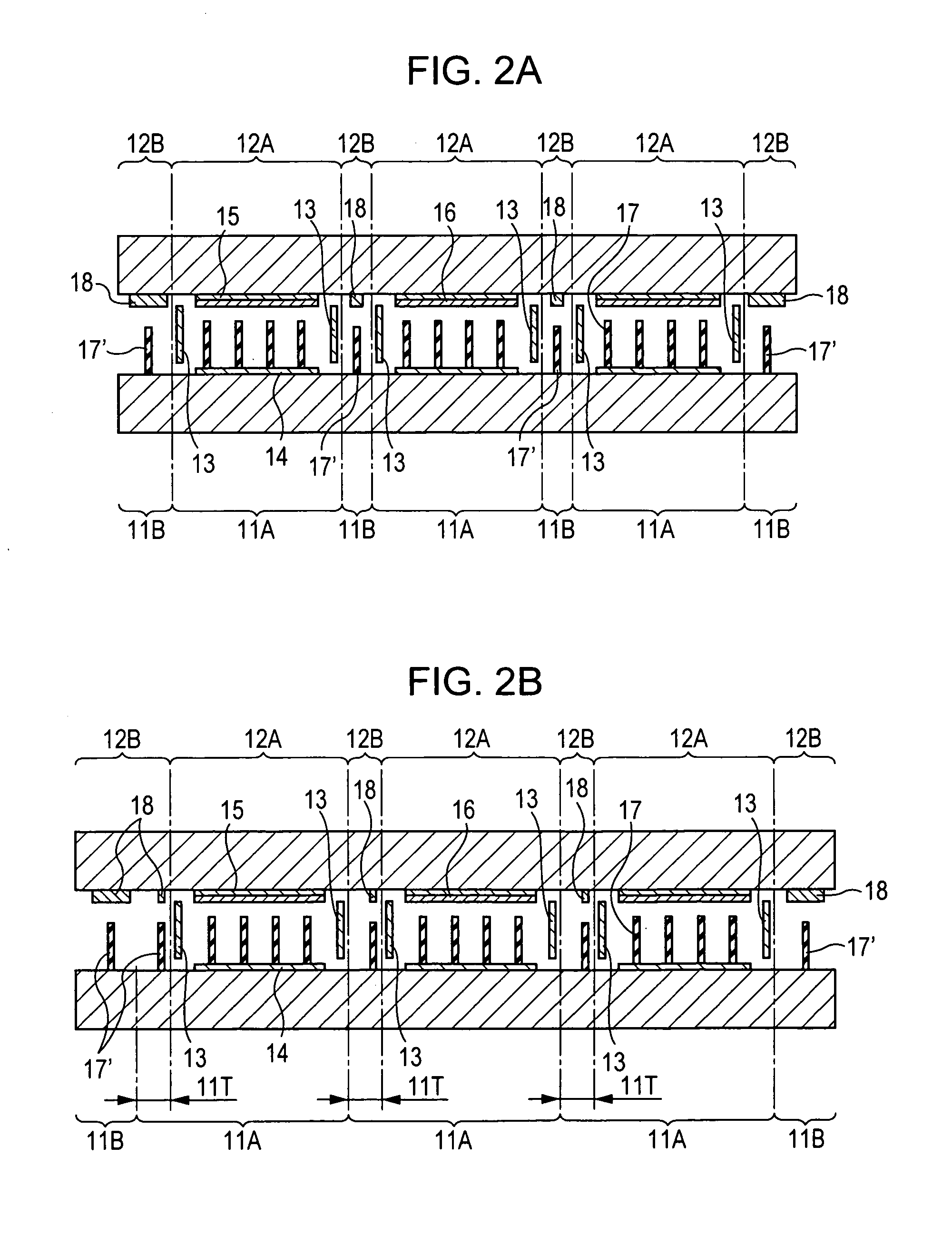
[0044]FIG. 1 is a schematic plan view schematically showing a pre-panel structure formed in the manufacturing method according to the embodiment, FIG. 2A is a schematic sectional view schematically showing a sectional structure taken along line IIA-IIA in FIG. 1, and FIG. 2B is a schematic sectional view schematically showing a sectional structure taken along line IIB-IIB in FIG. 1. In each of the attached drawings, the thickness of each layer and thin film, and the dimensions of a spacer are shown as being significantly larger than the thickness of a substrate for convenience of drawing and description, and are different from the actual dimensions. FIGS. 2A and 2B each schematically show the sectional structure of a pre-panel structure 10 before bonding.

[004...


PUM

PropertyMeasurementUnit
widthaaaaaaaaaa
thicknessaaaaaaaaaa
thicknessaaaaaaaaaa

Abstract

A method for manufacturing an electro-optic device having a panel structure including an electro-optic material disposed between a pair of substrates, a spacer disposed between the pair of substrates to define the gap therebetween, and a color filter provided on one of the pair of substrates includes forming a substrate region to be used as the panel structure and a peripheral region to be separated from the substrate region on each of a pair of pre-substrates, bonding the pair of pre-substrates together to form a pre-panel structure, and dividing the pre-panel structure to form the panel structure, wherein a stacked structure including the spacer and a colored layer constituting the color filter or a protective film covering the color filter is disposed in the peripheral region of the pre-panel structure.

Description

BACKGROUND OF THE INVENTION [0001] 1. Technical Field [0002] The present invention relates to a method for manufacturing an electro-optic device and an electro-optic device, and particularly relates to a technique for manufacturing an electro-optic device comprising a color filter and an electro-optic material provided between a pair of substrates, and a spacer for defining the space between the substrates. [0003] 2. Related Art [0004] Some electro-optic devices such as liquid crystal displays have a panel structure in which an electro-optic material is disposed between a pair of substrates. In many cases, a spacer is disposed between a pair of substrates, for defining the thickness of the electro-optic material. Known examples of a method for forming the panel structure comprising the spacer include a method in which a spacer comprising independent particles made of a synthetic resin is dispersed on one of a pair of substrates, and then the substrates are bonded together, and a met...

Claims


Application Information

Patent Timeline
Patent Type & Authority Applications(United States)
IPC IPC(8): G02F1/1333G02F1/1335G02F1/1339G09F9/00G09F9/30
CPCG02F1/1339G02F1/133351
Inventor KAMIJIMA, MOTOHIROTAGUCHI, SATOSHIASADA, KOJIIBUKI, SHINYAMARUYAMA, KUNIO
Owner SEIKO EPSON CORP
Why Eureka
Try Eureka