Methods and systems for lithography process control

a technology of lithography process and process control, applied in the direction of semiconductor/solid-state device testing/measurement, printing, instruments, etc., can solve the problems of low feature size which may be successfully fabricated, performance characteristics such as resolution capability of lithography process may often be limited, and variations in the dimensions of features at various times, so as to improve not only yield, but also high margin product yield

Inactive Publication Date: 2006-01-17
KLA TENCOR TECH CORP
View PDF69 Cites 144 Cited by
  • Summary
  • Abstract
  • Description
  • Claims
  • Application Information

AI Technical Summary

Benefits of technology

[0017]A further embodiment relates to a method for fabricating a semiconductor device. For example, the method may include measuring at least one property of a resist disposed upon a wafer during a lithography process. The method may also include altering at least one parameter of at least one process module in response to at least the one measured property of the resist to reduce within wafer variation of a critical metric of the lithography process. In addition, the method may include processing the wafer to form at least a portion of at least one semiconductor device upon the wafer. For example, processing the wafer may include etching, ion implantation, deposition, chemical mechanical polishing, or plating. In this manner, semiconductor devices formed by the method may have higher performance bin distributions thereby improving not only yield but also high margin product yield.

Problems solved by technology

As the features sizes of semiconductor devices continue to shrink, the minimum feature size which may be successfully fabricated may often be limited by performance characteristics of a lithography process.
In optical lithography, performance characteristics such as resolution capability of the lithography process may often be limited by the quality of the resist application, the performance of the resist, the exposure tool, and the wavelength of light which is used to expose the resist.
Furthermore, variations in temperature across a bake plate of a post exposure bake process module may cause variations in the dimensions of the features at various positions on a wafer.
There are several disadvantages, however, in using currently available methods to improve the resolution capability of lithography processes.
For example, currently available methods may not account for degradation in the uniformity of a critical parameter over time.
For a post exposure bake module, thermal relaxation of heating elements, contamination, or other performance variations may adversely affect the resolution capability of a lithography process to various degrees over time.
In this manner, systematic variations in the resolution capability from field to field across a wafer may not be monitored or altered, which may have an adverse affect on the overall performance characteristics of a lithography process.

Method used


Image

  • Methods and systems for lithography process control
  • Methods and systems for lithography process control
  • Methods and systems for lithography process control

Examples


Embodiment Construction

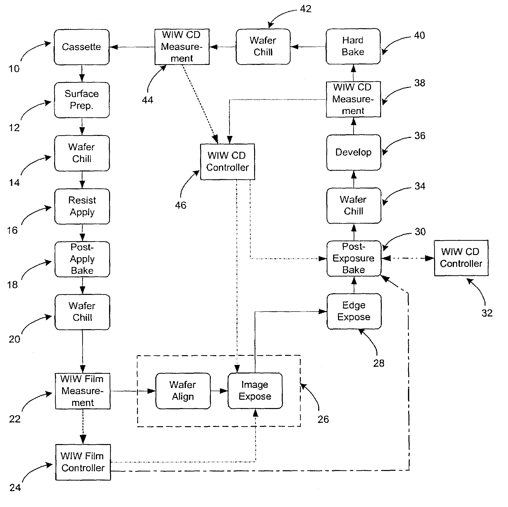
[0022]Turning now to the drawings, FIG. 1 illustrates an embodiment of a method to evaluate and control performance characteristics of a lithography process. For example, the method may be used to reduce, and even to minimize, within wafer (“WIW”) variability of critical metrics of the lithography process. Critical metrics of a lithography process may include, but are not limited to, critical dimensions of features formed by the lithography process and overlay. Critical dimensions of features formed during the lithography process may include, for example, a width, a height, and a sidewall profile of the features. A sidewall profile of a feature may be described, for example, by a sidewall angle of the feature with respect to an upper surface of a wafer, a roughness of the sidewall of the feature, and other physical characteristics of the feature. Overlay generally refers to a lateral position of a feature on one level of a wafer with respect to a lateral position of a feature on ano...


PUM

PropertyMeasurementUnit
temperatureaaaaaaaaaa

Abstract

Methods and systems for evaluating and controlling a lithography process are provided. For example, a method for reducing within wafer variation of a critical metric of a lithography process may include measuring at least one property of a resist disposed upon a wafer during the lithography process. A critical metric of a lithography process may include, but may not be limited to, a critical dimension of a feature formed during the lithography process. The method may also include altering at least one parameter of a process module configured to perform a step of the lithography process to reduce within wafer variation of the critical metric. The parameter of the process module may be altered in response to at least the one measured property of the resist.

Description

PRIORITY CLAIM[0001]This application is a continuation of and claims priority to U.S. patent application Ser. No. 09 / 849,622 filed May 4, 2001, now U.S. Pat. No. 6,689,519 which claims priority to U.S. Provisional Application No. 60 / 202,372 entitled “Method and System for Lithography Process Control,” filed May 4, 2000.BACKGROUND OF THE INVENTION[0002]1. Field of the Invention[0003]This invention generally relates to systems and methods for evaluating and controlling semiconductor fabrication processes. Certain embodiments relate to systems and methods for evaluating and / or controlling a lithography process by measuring a property of a resist and controlling a process step involved in the lithography process.[0004]2. Description of the Related Art[0005]Semiconductor fabrication processes typically involve a number of lithography steps to form various features and multiple levels of a semiconductor device. Lithography involves transferring a pattern to a resist formed on a semiconduc...

Claims


Application Information

Patent Timeline
Patent Type & Authority Patents(United States)
IPC IPC(8): G01B11/24G03F7/20H01L21/027H01L21/66
CPCG01N21/47G01N21/956G03F7/70558G03F7/70625G03F7/70641H01L22/20Y10S414/135H01L2924/0002H01L2924/00
Inventor LAKKAPRAGADA, SURESHBROWN, KYLE A.HANKINSON, MATTLEVY, ADY
Owner KLA TENCOR TECH CORP
Why Eureka
Try Eureka