Display device

a technology of display device and display screen, which is applied in the direction of static indicating device, non-linear optics, instruments, etc., can solve the problems of screen burn-in, high cost, and high cost, and achieve the effect of reducing adverse effects on display and minimizing the potential of data lines

Inactive Publication Date: 2005-11-24
SANYO ELECTRIC CO LTD
View PDF9 Cites 10 Cited by
  • Summary
  • Abstract
  • Description
  • Claims
  • Application Information

AI Technical Summary

Benefits of technology

[0010] According to the present invention, changing the voltage value of the difference between a first level and a second level in a storage capacitor line enables the contrast and screen brightness to be adjusted.
[0012] Furthermore, the capacitances generated at the locations where the two storage capacitor lines and the data lines intersect are set to be substantially the same. For this reason, during the voltage inversion of the two storage capacitor lines, fluctuations in the potential of the data lines can be minimized so as to reduce adverse effects on the display.

Problems solved by technology

It is well known that when a DC voltage is continuously applied across electrodes formed on opposing surfaces of the substrates, the alignment of the liquid crystal molecules becomes fixed, namely, the problem of screen burn-in occurs.
However, a problem was that its driving method is likely to become complex.

Method used


Image

  • Display device
  • Display device
  • Display device

Examples


specific example

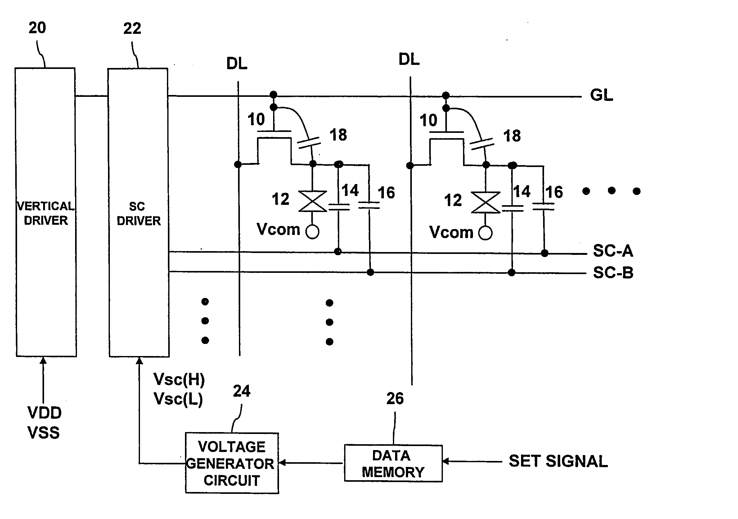
[0052] When configured so that Csc=320fF, Cpa=10fF, Clc=430fF, Cgs=3fF, ΔVsc=5.58, VB=3.5V, Vb=2.5V, and VDD=8.5V:

{(320−Cpa) / (3+430+320+Cpa)}·ΔVsc=3.5−2.5 / 2

Furthermore:

ΔVsc<8.5

[0053] Therefore, in this case, Cpa16.

[0054] For example, when Cpa is greater than or equal to 95fF and this condition is not satisfied, the shift voltage becomes insufficient and the black level display is not performed properly.

[0055] Furthermore, the voltage value Vpixel of the pixel electrode of the liquid crystal element 12 subsequent to shifting can be expressed as follows (identical to expression (1) given above):

Vpixel=Vvideo±{(Csc−Cpa} / (Cgs+Clc+Csc+Cpa)}·ΔVsc

[0056] When Cgs and Cpa are substantially smaller than Csc and Clc, Vpixel can be expressed as follows:

Vpixel□Vvideo±Csc / (Clc+Csc)·ΔVsc

[0057] Furthermore, the molecules in the TN liquid crystal are aligned in parallel with respect to the electrodes in the state where voltage is not applied, at which time the dielectric constant ε / / is s...


PUM

PropertyMeasurementUnit
voltageaaaaaaaaaa
voltagesaaaaaaaaaa
brightnessaaaaaaaaaa

Abstract

The level of a storage capacitor line changes between two types, an H level and an L level. As a result of this change, the voltage applied to a liquid crystal is shifted so that a sufficient voltage is applied to the liquid crystal to perform a display operation. Then, by changing the voltage value of the difference between a first level and a second level, the contrast and screen brightness are adjusted. Furthermore, the capacitances generated at the locations where the two storage capacitor lines and the data line intersect are set to be substantially the same.

Description

CROSS-REFERENCE TO RELATED APPLICATION [0001] The entire disclosure of Japanese Patent Application Nos. 2004-152485, 2004-152489, 2004-152493, and 2004-152497 including specification, claims, drawings and abstract is incorporated herein by reference. BACKGROUND OF THE INVENTION [0002] 1. Field of the Invention [0003] The present invention relates to a display device having display circuits arranged in a matrix configuration. [0004] 2. Description of the Related Art [0005] Conventionally, liquid crystal display devices are known as low power consumption display devices that can assume a thinner and more lightweight form and are employed in various types of equipment as display devices. Liquid crystal display devices (hereinafter referred to as LCD) have two substrates with electrodes formed on opposing sides thereof, laminated with liquid crystals injected between them. A display operation is performed by applying a voltage signal across the electrodes to control the alignment of the...

Claims


Application Information

Patent Timeline
Patent Type & Authority Applications(United States)
IPC IPC(8): G02F1/1362G09G3/36
CPCG02F1/1362G02F1/133
Inventor SENDA, MICHIRUHIROSAWA, KOJIYOKOYAMA, RYOICHI
Owner SANYO ELECTRIC CO LTD
Why Eureka
Try Eureka