

Substrate treatment method and substrate treatment apparatus
a substrate treatment and substrate technology, applied in the direction of coatings, basic electric elements, chemical vapor deposition coatings, etc., can solve the problems of increasing the amount of resist solution going to waste, and reducing the total consumption of treatment solution. , the effect of reducing the number of pre-dispenses
- Summary
- Abstract
- Description
- Claims
- Application Information
AI Technical Summary
Benefits of technology
Problems solved by technology
Method used
Image

Examples
Embodiment Construction
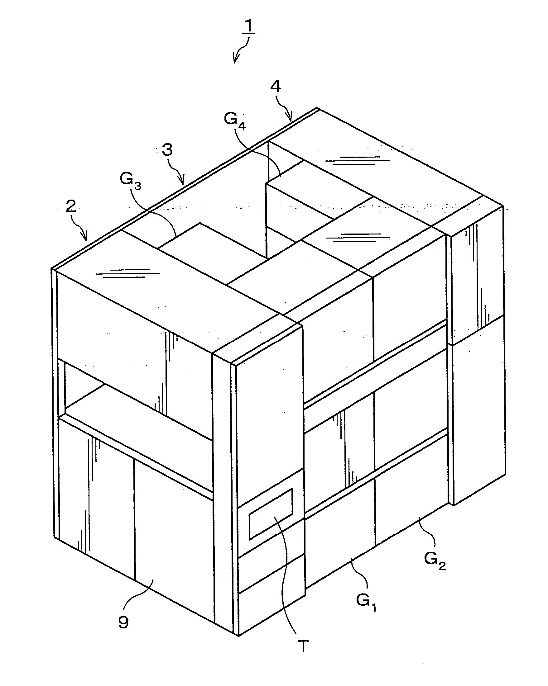
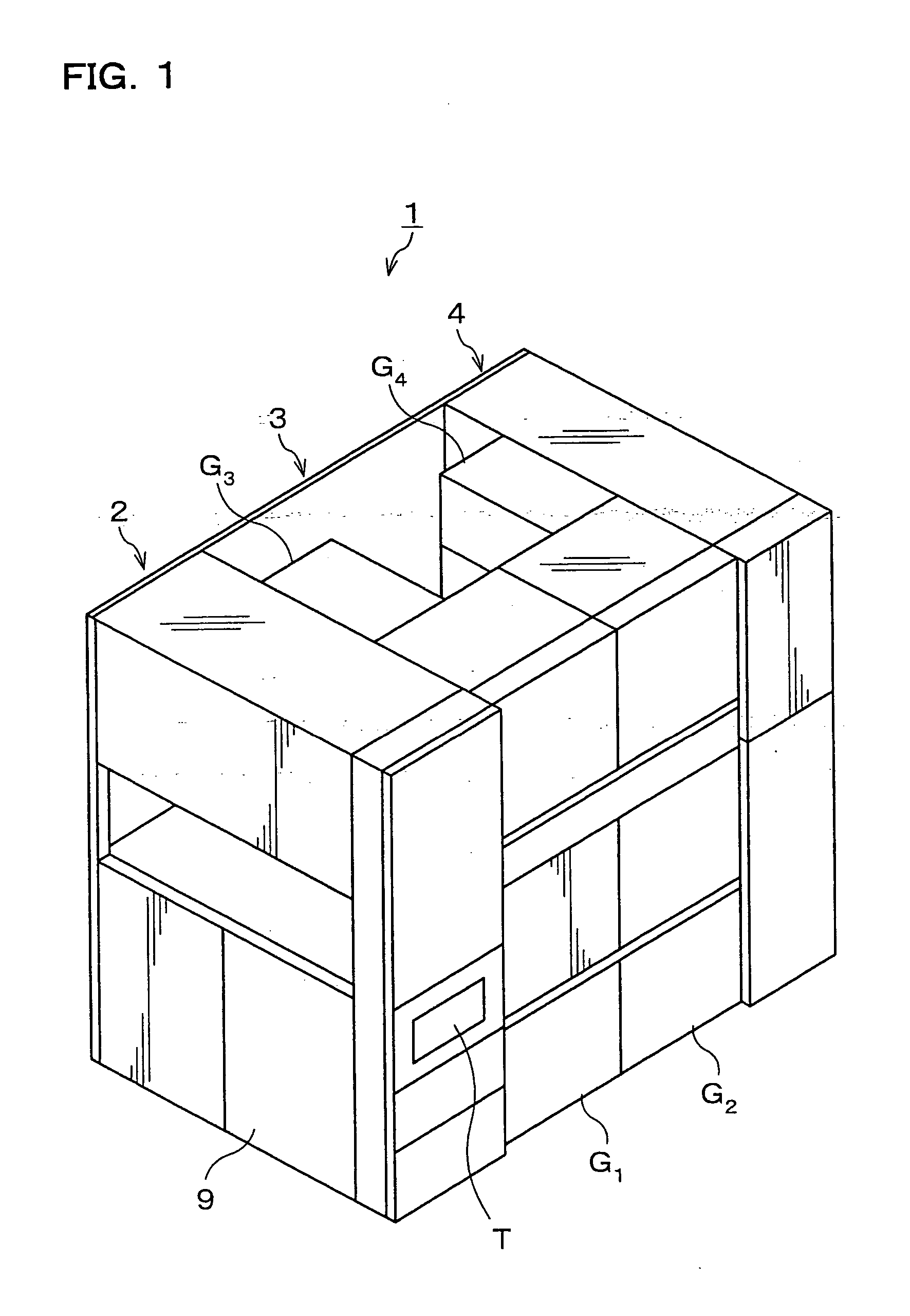
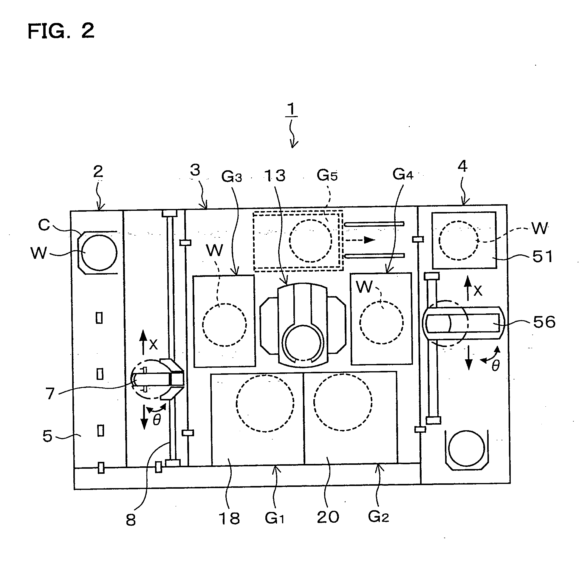
[0035] Hereinafter, preferred embodiments of the present invention will be described. FIG. 1 is a perspective view of a coating and developing treatment system 1 capable of implementing a substrate treatment method according to the this embodiment, and FIG. 2 is a plane view schematically showing the configuration of the coating and developing treatment system 1.
[0036] As shown in FIG. 1 and FIG. 2, the coating and developing treatment system 1 has a configuration in which a cassette station 2 for carrying, for example, 25 wafers W in a unit of cassette from / to the outside to / from the coating and developing treatment system 1 and for carrying the wafers W to / from a cassette C, a processing station 3 composed of various kinds of processing units which are disposed in multi-tiers, for performing predetermined processing for the wafers W one by one in coating and developing processes, and an interface section 4 for delivering / receiving the wafers W to / from an aligner (not-shown) which...
PUM
| Property | Measurement | Unit |
|---|---|---|
| Time | aaaaa | aaaaa |
Abstract
Description
Claims
Application Information