Nonvolatile memory cells having high control gate coupling ratios using grooved floating gates and methods of forming same

a technology of nonvolatile memory and control gate, which is applied in the direction of semiconductor devices, electrical devices, transistors, etc., can solve the problems of adversely affecting the coupling ratio and the loss of stored data of devices

Inactive Publication Date: 2005-11-24
SAMSUNG ELECTRONICS CO LTD
View PDF9 Cites 40 Cited by
  • Summary
  • Abstract
  • Description
  • Claims
  • Application Information

AI Technical Summary

Problems solved by technology

Volatile memory devices lose stored data when power is interrupted, whereas nonvolatile memory devices retain stored data even if the power is abruptly interrupted.
The flash memory cell shown in FIG. 1 may improve the integration density of an electronic system, but the inter-gate dielectric layer 116 around the floating gate 115 may adversely affect the coupling ratio.

Method used


Image

  • Nonvolatile memory cells having high control gate coupling ratios using grooved floating gates and methods of forming same
  • Nonvolatile memory cells having high control gate coupling ratios using grooved floating gates and methods of forming same
  • Nonvolatile memory cells having high control gate coupling ratios using grooved floating gates and methods of forming same

Examples


Embodiment Construction

[0024] The present invention will now be described more fully hereinafter with reference to the accompanying drawings, in which exemplary embodiments of the invention are shown. This invention may, however, be embodied in different forms and should not be construed as limited to the embodiments set forth herein. Rather, these embodiments are provided so that this disclosure is thorough and complete and fully conveys the scope of the invention to those skilled in the art. In the drawings, the thickness of layers and regions are exaggerated for clarity. The same reference numerals are used to denote the same elements.

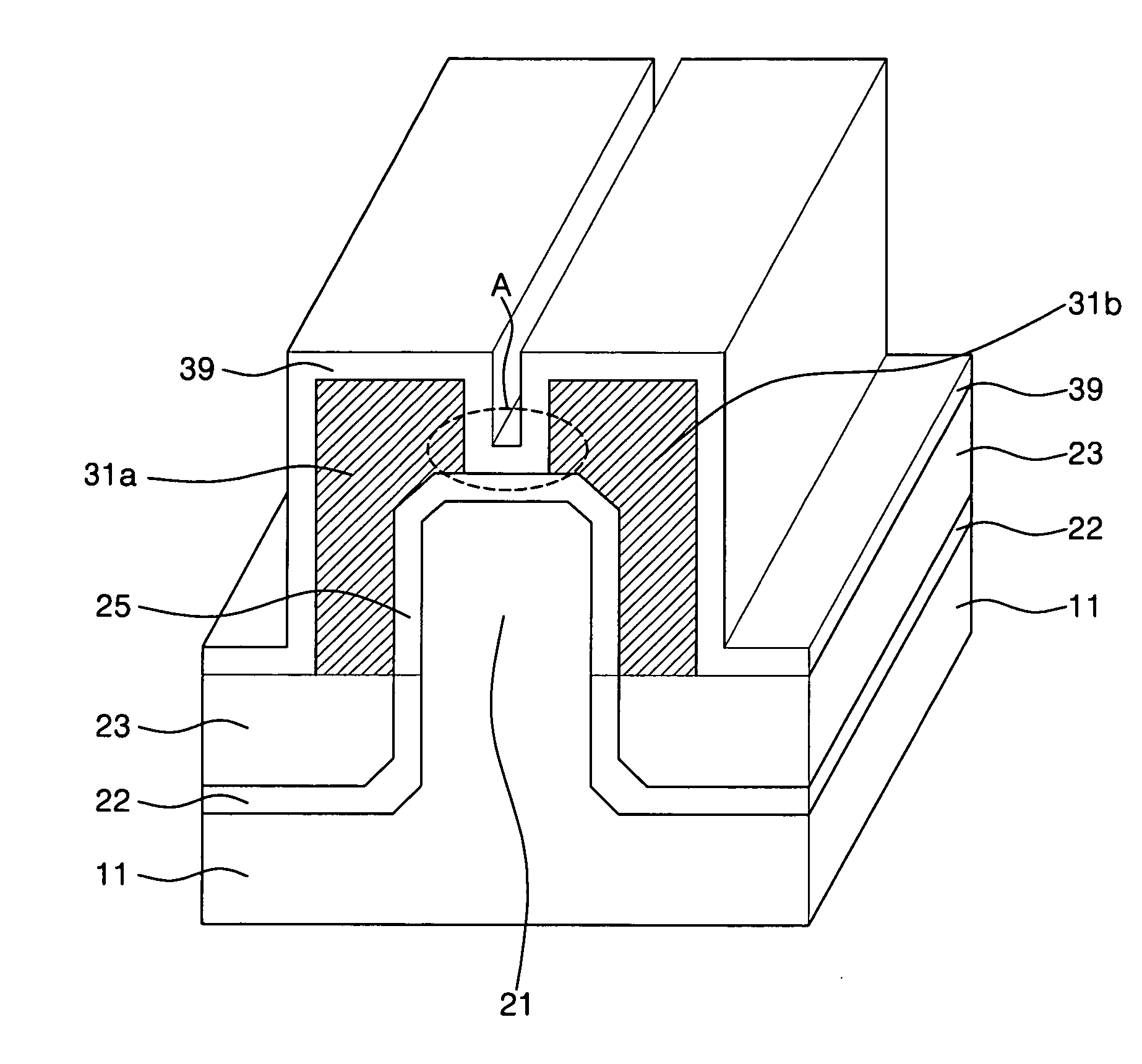
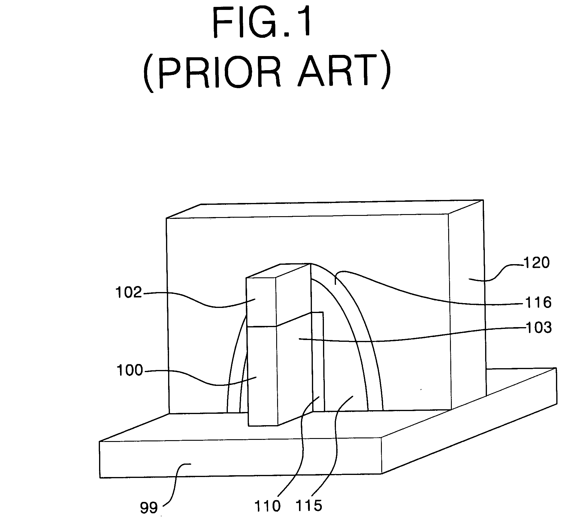
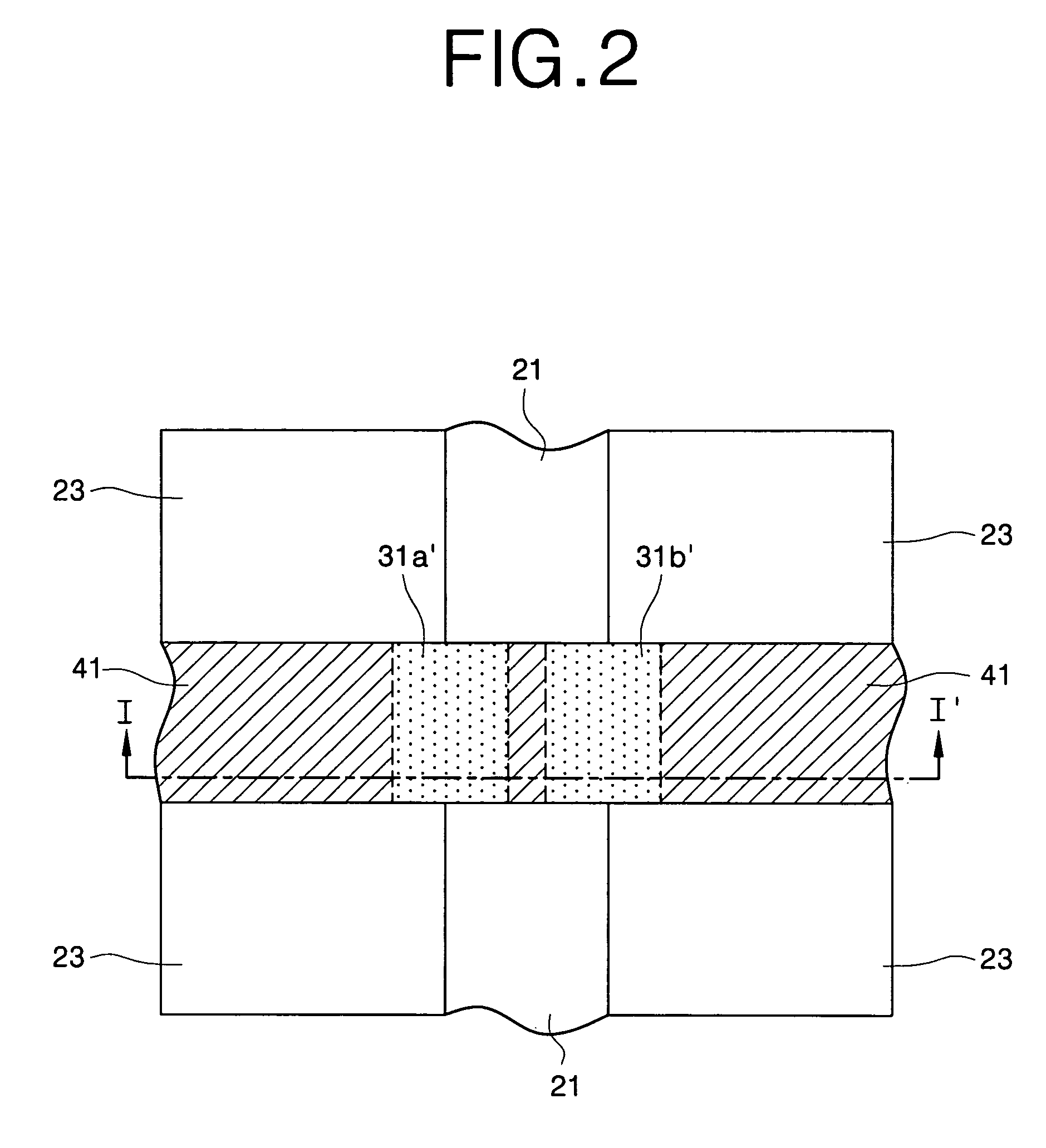
[0025]FIGS. 2 through 12 include a plan view, cross-sectional views, and perspective views illustrating a flash memory cell having a floating gate and method of fabricating the same according to an exemplary embodiment of the present invention. Specifically, FIG. 2 is a plan view of a portion of the flash memory cell, FIGS. 3, 5, 6, 7, 8, 9, and 11 are cross-sectional vi...


PUM


Abstract

A non-volatile memory cell includes a semiconductor substrate having a fin-shaped active region extending therefrom. A tunnel dielectric layer is provided, which extends on opposing sidewalls and an upper surface of the fin-shaped active region. A floating gate electrode is provided on the tunnel dielectric layer. This floating gate electrode has at least a partial groove therein. An inter-gate dielectric layer is also provided. This inter-gate dielectric layer extends on the floating gate electrode and into the at least a partial groove. A control gate electrode is provided, which extends on the inter-gate dielectric layer and into the at least a partial groove.

Description

REFERENCE TO PRIORITY APPLICATION [0001] This application claims priority to Korean Patent Application No. 2004-37050, filed May 24, 2004, and Korean Patent Application No. 2004-39374, filed May 31, 2004, the disclosures of which are hereby incorporated herein by reference. FIELD OF THE INVENTION [0002] The present invention relates to memory device and methods of forming memory devices and, more particularly, to nonvolatile memory devices and methods of forming nonvolatile memory devices. BACKGROUND OF THE INVENTION [0003] Semiconductor memory devices that store data can be categorized as either volatile memory devices or nonvolatile memory devices. Volatile memory devices lose stored data when power is interrupted, whereas nonvolatile memory devices retain stored data even if the power is abruptly interrupted. Nonvolatile memory devices include flash memory devices. A unit cell of a conventional flash memory device (hereinafter, referred to as a “flash memory cell”) can include an...

Claims


Application Information

Patent Timeline
Patent Type & Authority Applications(United States)
IPC IPC(8): H01L21/28H01L21/3205H01L21/336H01L29/423H01L29/786H01L29/788
CPCH01L21/28273H01L21/28282H01L29/42324H01L29/7881H01L29/66825H01L29/7851H01L29/7853H01L29/66787H01L29/40114H01L29/40117
Inventor CHO, EUN-SUKLEE, CHOONG-HOKIM, TAE-YONG
Owner SAMSUNG ELECTRONICS CO LTD
Why Eureka
Try Eureka