Enhanced blind hole termination of pin to PCB

Inactive Publication Date: 2005-12-01
ITT MFG ENTERPRISES INC
View PDF6 Cites 9 Cited by
  • Summary
  • Abstract
  • Description
  • Claims
  • Application Information

AI Technical Summary

Benefits of technology

[0005] In accordance with one embodiment of the present invention, a solder connection is provided between a lead or tail of a component lying on a multi-layer circuit board arrangement and a plating on the arrangement, and a method for producing such solder connection, which avoids the high capacitance loading, low shear and tension strength, and the need for resilient or precision tails of the prior art. In a multi-board arrangement, a blind hole is formed that extends through only a portion of the thickness of a multi-layer circuit board. The blind hole is plated to form a solder well whose bottom is formed by the bottom of the hole. The tail of a component is inserted down into the hole and soldered in place thereat, as by a solder paste that was previously placed in the well or around the tail. The portion of the tail lying in the circuit board is short, being less than the thickness of the multi-layer board, to avoid a significant capacitive load. However, a considerable length of the tail, such as a length that is about equal to its diameter, is firmly soldered in and above the hole, so the tail resists considerable force tending to break the solder connection. The tails do not have to be formed with high precision, since a rugged connection is achieved with tails that project different distances into the solder wells.

Problems solved by technology

This results in considerable capacitance between the plated walls of the hole and close traces on the laminates, or layers of the assembly, and results in increased crosstalk and decreased signal strength.
The SMT technique results in solder joints that are mechanically weak against shear forces that tend to move the tails parallel to the plane of the board upper face and against pull up forces.

Method used


Image

  • Enhanced blind hole termination of pin to PCB
  • Enhanced blind hole termination of pin to PCB
  • Enhanced blind hole termination of pin to PCB

Examples


Embodiment Construction

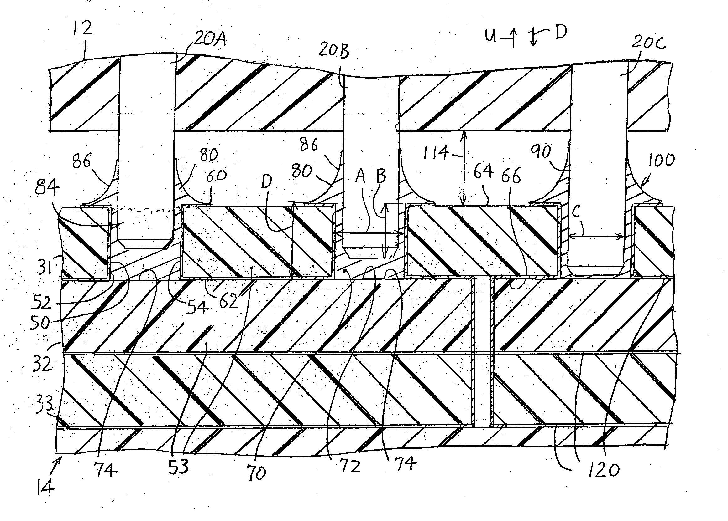
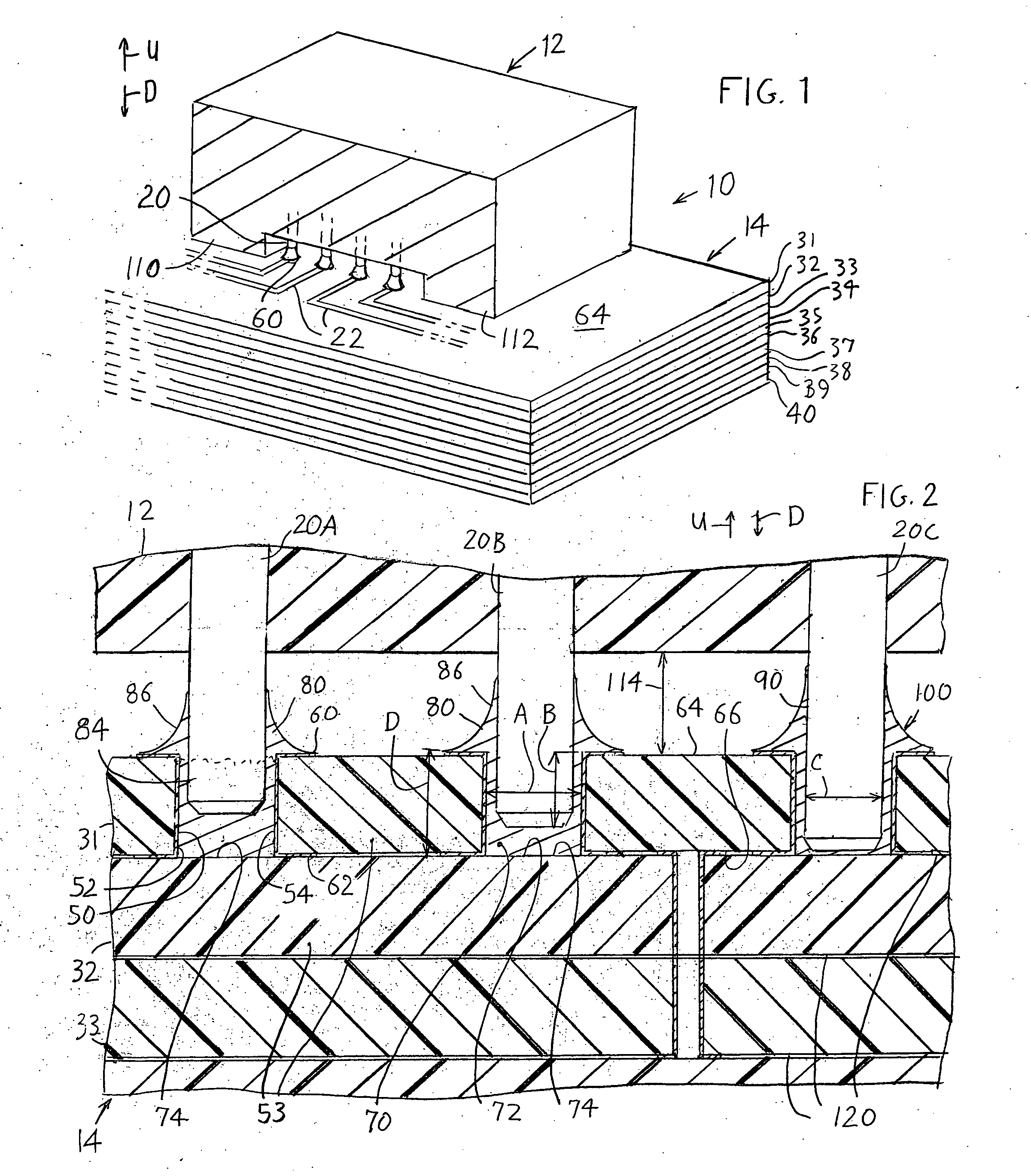
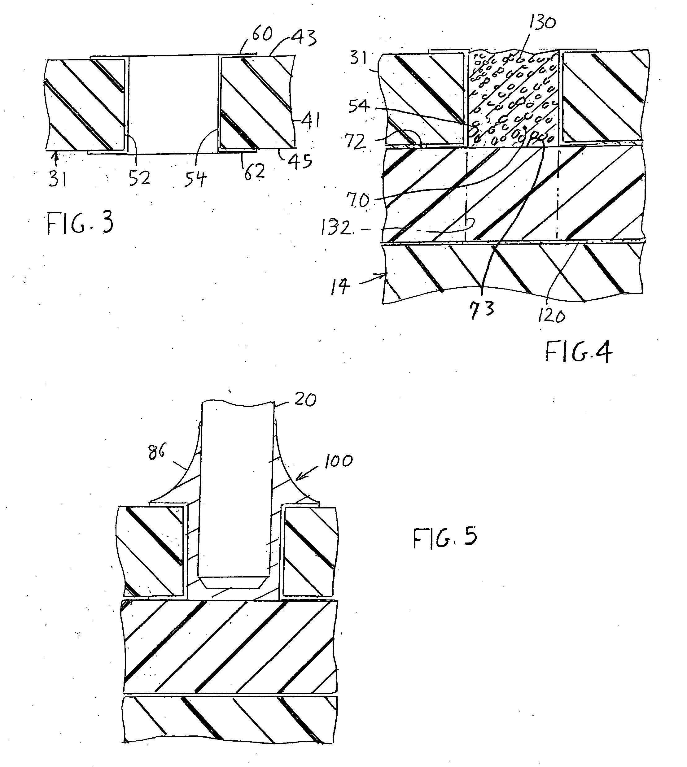
[0013]FIG. 1 illustrates a termination system 10 of the present invention, wherein a component 12 that lies on a multi-layer circuit board assembly 14 has component pins, or leads, or tails 20 that must be soldered to traces 22 on a first layer 31 of the circuit board assembly. The particular circuit board assembly 14 includes ten layers 31-40 that lie in a facewise stack wherein each layer lies facewise adjacent to one or two other layers, to form a facewise stack of layers. Up and down directions are indicated by arrows U and D for the particular orientation of the component and board assembly illustrated in the figures, although it should be understood that the board assembly and component can lie in any orientation. As shown in FIG. 3, each layer such as 31 includes a plate 41 of insulative material. Most or all of the layers also include traces such as 60, 62 on one or both faces 43, 45 of the plate, the traces being formed of a film of conductive material.

[0014]FIG. 2 shows t...


PUM


Abstract

Tails (20) projecting from an electrical component (12) that lies on a circuit board surface, are terminated to traces on a multi-layer circuit board (14) in a manner that minimizes the disadvantages of long through hole soldering and of surface mount techniques. A blind hole is drilled and plated to form a shallow well (70). The well is filled with a soldering composition (130). A tail (20) is projected downward into the soldering composition with the extreme tip of the tail lying above the bottom of the hole, and the soldering composition is heated to solder the tail to the hole plating.

Description

CROSS-REFERENCE [0001] This is a continuation-in-part of U.S. patent application Ser. No. 10 / 461,840 that was filed Jun. 13, 2003.BACKGROUND OF THE INVENTION [0002] Components that lie on a circuit board typically have leads or tails that must be soldered to traces on the circuit board. One technique for mounting the tails includes drilling holes through the circuit board, plating the holes and then fixing the tails in the holes. The tail can be a compliant pin which is forced into the hole in an interference fit, or can be soldered in place with the solder joined to tail portions that project from opposite ends of the hole. When a multi-layer circuit board assembly is used, the through holes extending the board assembly are long and tails to be soldered in the holes must be long. This results in considerable capacitance between the plated walls of the hole and close traces on the laminates, or layers of the assembly, and results in increased crosstalk and decreased signal strength....

Claims


Application Information

Patent Timeline
IPC IPC(8): H05K1/11H05K3/34H05K3/46
CPCH05K1/112H05K3/3421H05K3/4614H05K3/4623H05K2201/09472Y10T29/49156H05K2201/09536H05K2201/10704Y10T29/49155Y10T29/49144Y10T29/49165H05K2201/09509
Inventor MICKIEVICZ, SCOTT KEITHKNAUB, JOHN EDWARD
Owner ITT MFG ENTERPRISES INC
Why Eureka
Try Eureka