

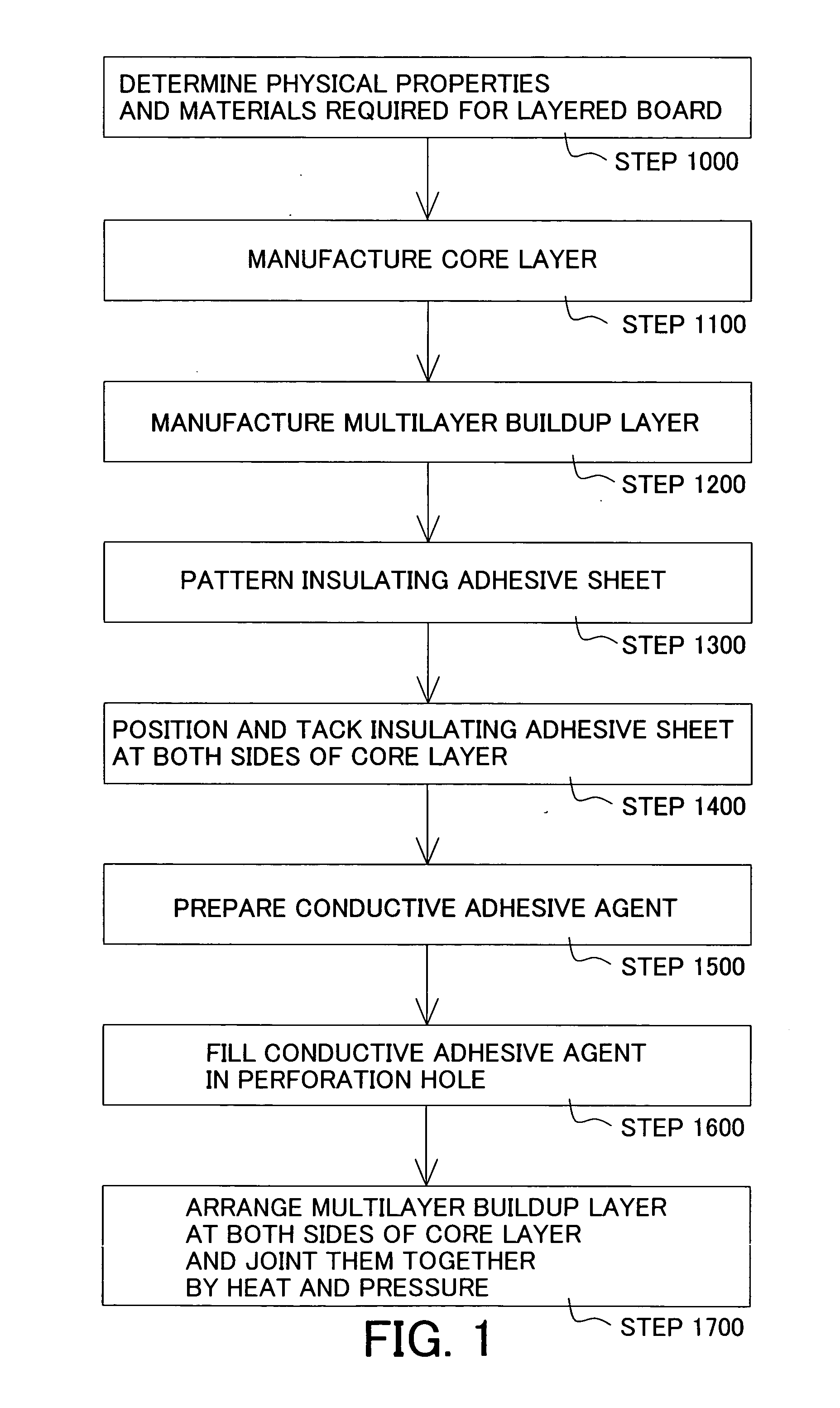
Layered board and manufacturing method of the same, electronic apparatus having the layered board
a manufacturing method and layering technology, applied in the field of layering boards, can solve the problems of wasting non-defective core layer and buildup layer on the other side, unable to determine defective, and conventional manufacturing methods that have a bad yield of buildup boards, etc., to achieve the effect of improving yield
- Summary
- Abstract
- Description
- Claims
- Application Information
AI Technical Summary
Benefits of technology
Problems solved by technology
Method used
Image

Examples
example 1
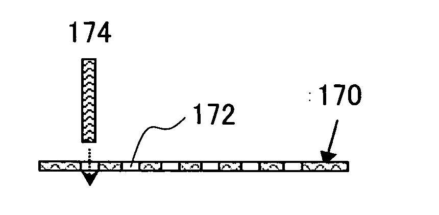
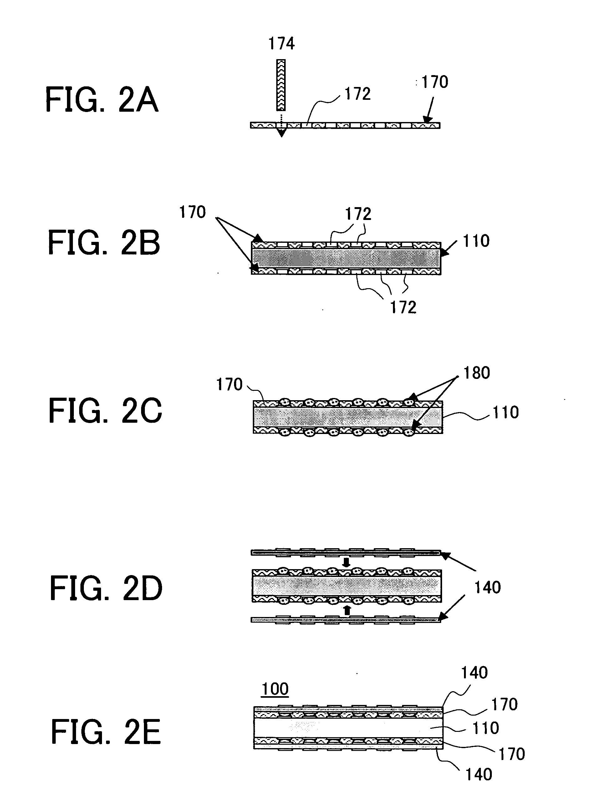
[0080] First, desired coefficient of thermal expansion and modulus of longitudinal elasticity are set to 3 ppm / ° C. and 55 GPa. When the coefficients of thermal expansion of the core layer 110 and the buildup layer 140 were 1 ppm / ° C. and 20 ppm / ° C., respectively, their thicknesses were set to 3 mm and 0.2 mm, and their moduli of longitudinal elasticity were set to 56 GPa and 48 GPa, the layered board 100 could have designed coefficient of thermal expansion and modulus of longitudinal elasticity.
[0081] The conductive adhesive 180 of the present invention is broadly applicable to joints of two members having different coefficients of thermal expansion in an electronic apparatus. For example, these two members are an exoergic circuit device, such as a CPU, and a transmission member, such as a heat spreader and a heat sink, which transmits the heat from the exoergic circuit device. This structure can lower the temperature for junction, and prevents remelting when the exoergic circuit...
PUM
| Property | Measurement | Unit |
|---|---|---|
| thickness | aaaaa | aaaaa |
| thickness | aaaaa | aaaaa |
| thickness | aaaaa | aaaaa |
Abstract
Description
Claims
Application Information