

Organic thin film transistor and flat panel display comprising the same
- Summary
- Abstract
- Description
- Claims
- Application Information
AI Technical Summary
Benefits of technology
Problems solved by technology
Method used
Image

Examples
Embodiment Construction
[0035] The present invention will now be described more fully with reference to the accompanying drawings showing exemplary embodiments of the invention.
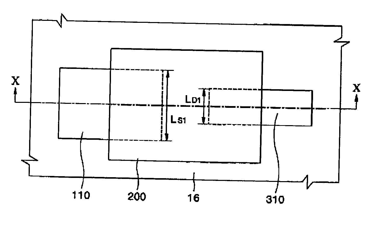
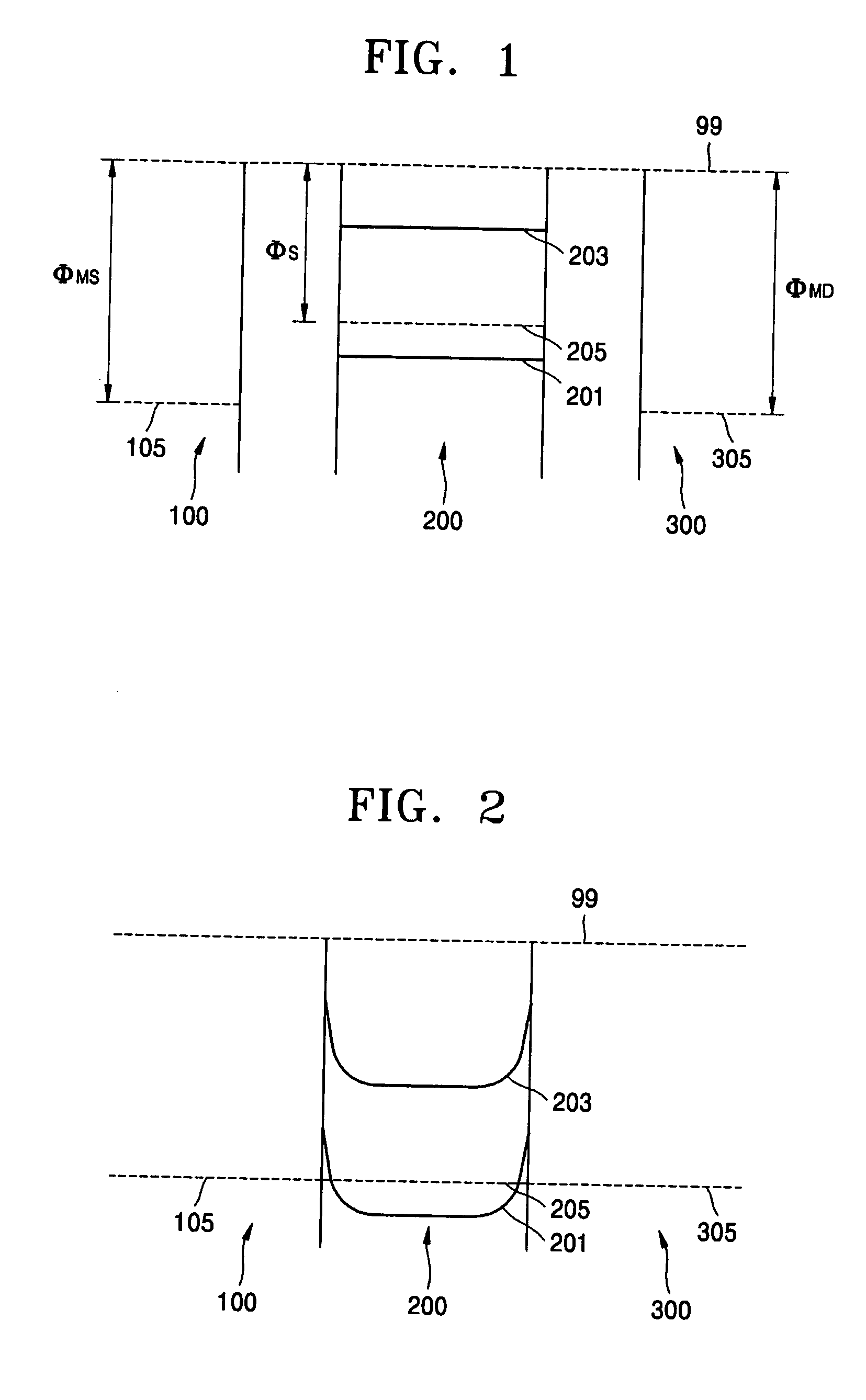
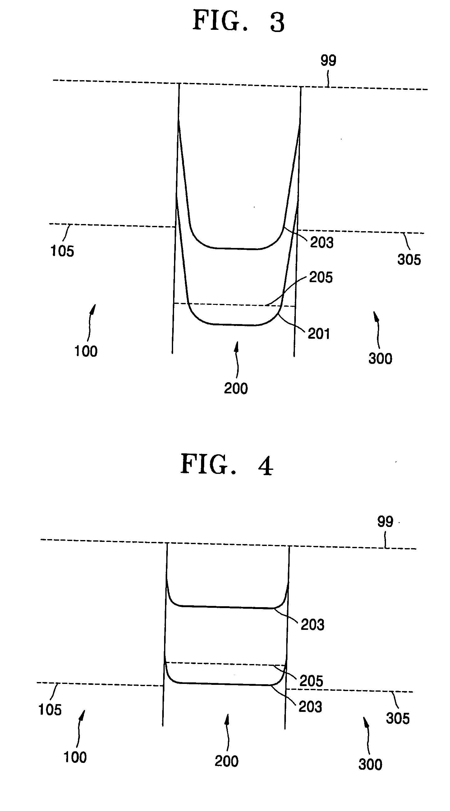
[0036]FIG. 1 is a conceptual drawing showing energy band diagrams of a source electrode 100, a P-type organic semiconductor layer 200, and a drain electrode 300 before contacting each other. Hereinafter, an organic TFT having the P-type organic semiconductor layer 200 will be described, but the present invention is not limited thereto. Rather, it may also be applied to an organic TFT having different types of organic semiconductor layers.
[0037] Referring to FIG. 1, the energy differences between a vacuum energy level 99 and the Fermi energy levels 105 and 305 of the source electrode 100 and the drain electrode 300 are the source and drain electrodes' work functions φMS and φMD, respectively. The energy difference between the vacuum energy level 99 and the Fermi energy level 205 of the P-type organic semiconductor layer 200 is the ...
PUM
 Abstract
Description
Claims
Application Information