Optical device

a technology of optical modulator and optical waveguide, which is applied in the field of optical elements, can solve the problems of limited size of the device using the optical modulator, increased production cost, and increased size of the optical modulator

Active Publication Date: 2005-12-08
SUMITOMO OSAKA CEMENT CO LTD +1
View PDF4 Cites 21 Cited by
  • Summary
  • Abstract
  • Description
  • Claims
  • Application Information

AI Technical Summary

Problems solved by technology

These cause the optical modulator to grow in size, generating problems that the production costs get higher and that the size of the device using the optical modulator is limited.
Moreover, when several electrodes are placed on a limited size substrate, it is not possible to set the electrodes of enough length in relation to the arrangement of electrode.
The problems that the production costs get higher and the size of the device using the optical modulator is limited still remain unsolved.
Thus, chirping is generated in the modulated light wave from the optical element, and this could be a cause of limiting distance of transmission.
This setup could cause higher costs since adjustment of the electrical signals gets complicated and the number of components increases.
This could cause the problems that driving voltage increases and that chirping is generated as in FIG. 12.
This jumper lead could be a cause that propagation loss of the modulating signal dramatically increases.

Method used


Image

  • Optical device
  • Optical device
  • Optical device

Examples


second embodiment

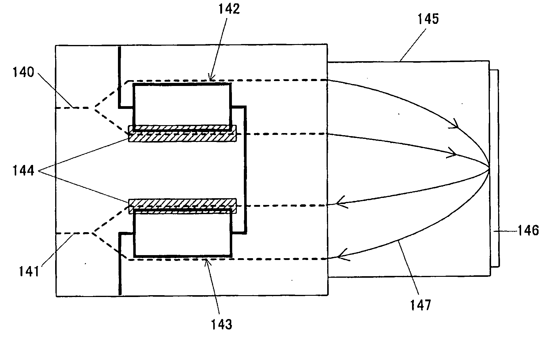
[0149]FIG. 18 shows the optical element using the branching and confluence lines according to the present invention, wherein MZ type optical waveguides 140 and 141 are turned back by a GRIN lens 145 and a reflecting mirror 146 attached to one side edge of said lens. The light wave exiting from an optical waveguide 140 at the input side follows the locus shown by 147 and enters an optical waveguide 141 at the output side. The modulating electrode having two branching and confluence lines 142 and 143 is placed on each optical waveguide 140 and 141 like FIG. 17. FSP reversal regions 144 are also formed on one part of each optical waveguide to be operated like FIG. 17.

third embodiment

[0150] Subsequently, the optical element using the branching and confluence lines according to the present invention is shown in FIG. 19.

[0151]FIG. 19 shows the optical waveguide where MZ type optical waveguides 150 and 151 are located in series on substrate 101. Using such several MZ type optical waveguides enables the light wave being optical-modulated in one MZ type optical waveguide to be again optical-modulated by another MZ type optical waveguide. Especially when it is modulated by the same modulating signal, it is possible to improve extinction ratio related to the modulation.

[0152] In FIG. 19, two branching and confluence lines 152 and 153 are located corresponding to the interaction part of each MZ type optical waveguide. FSP reversal regions 154 and 155 are also formed on one part of each branching optical waveguide. Because the single middle line connects each branching and confluence line 152 and 153, it becomes easy to wire the lines as well as it becomes possible to a...

fourth embodiment

[0154]FIG. 20 shows the optical element using the branching and confluence lines according to the present invention, wherein two MZ type optical waveguide of FIG. 19 are configured by the turnback. A reflecting mirror 166 is formed at the turnback. Branching and confluence lines 162 and 163, and FSP reversal regions 164 and 165 are formed on each MZ type optical waveguide 160 and 161. Further, it is also possible to form a delay line 167 for the purposes of adjusting the timing between the light wave entering the next MZ type optical waveguide 161 and the modulating signal.


PUM

PropertyMeasurementUnit
phaseaaaaaaaaaa
frequencyaaaaaaaaaa
electrical connectionaaaaaaaaaa

Abstract

The present invention provides a highly-integrated and compact optical element and further provides an optical element having various functions such as lower driving voltage, chirping suppression and polarization-independency.
The optical element comprising a substrate 1 consisting of a material having an electrooptic effect, top optical waveguides 2-1 an 2-2 formed on the top face of said substrate, bottom optical waveguides formed on the bottom face of said substrate, a top modulating electrode for controlling the phase of a light wave being propagated through said top optical waveguide, and a bottom modulating electrode for controlling the phase of a light wave being propagated through said bottom optical waveguide, is characterized in that at least one side edge of said substrate comprises output and input of said optical waveguides formed on said top and bottom faces, and a turnback element is located adjacent to said one side edge to guide the light wave from said output to said input.

Description

BACKGROUND OF THE INVENTION [0001] (1) Field of the Invention [0002] The present invention relates to an optical element, and in particular to an optical element wherein optical waveguides formed on different faces of the same substrate are optically connected. In addition, it relates to an optical element for applying the same modulating signal into different optical waveguides. [0003] (2) Related Art Statement [0004] In recent years, external optical modulators such as an optical waveguide device have been widely used in the field of optical communication or the like for the purpose of enabling high-speed switching. Optical waveguide modulators consisting of lithium niobate (LiNbO3; hereinafter referred to as LN), which have features of high frequency characteristic, low insertion loss, high extinction ratio or the like, and optical waveguides formed by thermal diffusion of Ti on said substrate, have been put to practical use. [0005] In improving or adding functions of the optical...

Claims


Application Information

Patent Timeline
Patent Type & Authority Applications(United States)
IPC IPC(8): G02F1/035G02F1/055G02F1/21G02F1/225
CPCG02F1/035G02F1/0356G02F1/055G02F1/21G02F1/225G02F2201/34
Inventor OIKAWA, SATOSHIICHIOKA, MASAYUKIICHIKAWA, JUNICHIROYAMAMOTO, FUTOSHIKURIMURA, SUNAOKITAMURA, KENJI
Owner SUMITOMO OSAKA CEMENT CO LTD
Why Eureka
Try Eureka