Conducting luminescent organic compounds

a luminescent organic compound and conductor technology, applied in the direction of non-metal conductors, cell components, conductors, etc., can solve the problems of inability to achieve sufficient molecular orientation, inability to use widely in practice, and decrease in the conduction path of charge carriers, etc., to achieve good solubility in solvents, impair the high field effect mobility, and facilitate the effect of mobility

Inactive Publication Date: 2005-12-15
FUJIFILM CORP
View PDF1 Cites 8 Cited by
  • Summary
  • Abstract
  • Description
  • Claims
  • Application Information

AI Technical Summary

Benefits of technology

[0009] The present invention is directed to solve the above problems in prior art techniques, and an object of the present invention is to provide an electrically conducting organic compound which can exhibit a high field effect mobility and at the same time, can be produced by a simple and easy process at a low cost.
[0011] Still another object of the present invention is to provide a high-performance electronic device having flexibility.
[0016] As described in detail below, accordingly to the present invention, a side chain substituent such as an alkyl group is introduced as a functional group into a condensed polycyclic aromatic compound in which the π-conjugate system is planarly extended and which has high mobility, such as ovalene, whereby good solubility in a solvent can be ensured and an electronic device having desired properties can be manufactured without impairing the high field effect mobility even by an easy process of forming a thin film from a solution system, such as casting or printing. Furthermore, by imparting a functionality to the functional group itself introduced into the condensed polycyclic aromatic compound, the molecules can be oriented at the time of coating and drying the aromatic compound. For example, by introducing a functional group having liquid crystallinity or a long-chain alkyl group, a desired molecular orientation can be attained.

Problems solved by technology

However, currently existing electronic circuits mainly comprising an inorganic material such as polycrystalline silicon or amorphous silicon require a large-scale process such as high temperature and high vacuum and, taking account of the heat resistance and high production cost of the plastic substrate, these circuits are applicable, at best, to only a part of an instrument and cannot be used widely in practice.
In the case of forming the film from a solution, the field effect mobility is usually further lower, by about 1 or 2 figures, due to the difficulty in controlling the molecular orientation.
In other words, a most important problem in realizing an organic semiconductor is how high field effect mobility can be achieved by a simple and easy production process.
However, the orientation force on an organic semiconductor by the orientation film is weak and, at present, a sufficiently high molecular orientation cannot be attained.
The introduction of a crystalline substituent incurs a problem such that the conduction path of the charge carrier is decreased due to the presence of the substituent not contributing to the electrical conductivity and the mobility is rather reduced.
The organic semiconductor where the π-conjugate system is planarly extended, such as pentacene, phthalocyanine and ovalene, has almost no solubility in a solvent and since the film is formed by vapor deposition, the cost is a great problem.

Method used


Image

  • Conducting luminescent organic compounds
  • Conducting luminescent organic compounds
  • Conducting luminescent organic compounds

Examples


examples of form

[0194] A4 size or more.

Examples of Function:

[0195] Receiving and sending, data memory, switchover of picture plane, enlargement / reduction, input, search, image input, etc.

Examples of Constituent Element:

[0196] Display part, driving circuit, power source, communication (sending and receiving) circuit, control circuit, memory, input means, image input means, etc.

Examples of Application:

[0197]FIG. 17 shows an example of a display device for a global education system. The global education system as used herein includes an electronic blackboard 581 as the same display device as that of the electronic conference system of (7) and the same display device 582 as that of the electronic text of (19). By linking with schools around the world, the contents written on the electronic blackboard 581 by a teacher can be sent, displayed and recorded to the display device 582 of students. Individual communication between the teacher and a student can be supported. A voice input and output fu...

example 1

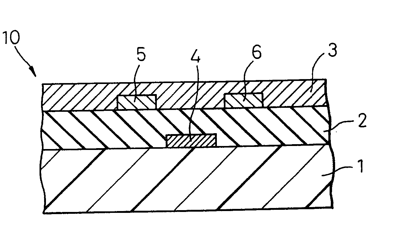
[0216] On a substrate plastic sheet comprising polyether sulfone, a gate electrode was formed by sputtering of gold, cyanoethylated pullulan dissolved in acetone was coated thereon, and then the solvent was dried to form an insulating layer having a film thickness of 150 nm. On this insulating layer, a source electrode and a drain electrode at an electrode-to-electrode distance, namely, a channel length, of 5 μm were each formed to a film thickness of 50 nm by sputtering of gold. On the plastic substrate with electrodes thus formed, an ovalene derivative having attached thereto a hexyl group (see, the following formula):

which was dissolved under heating in toluene was coated by spin coating and then, the solvent was gradually dried to obtain a channel layer having a film thickness of 100 nm.

[0217] Subsequently, for the thus-manufactured organic thin film transistor, the mobility of the electrically conducting organic compound was calculated from the relationships between the dra...

example 2

[0218] On a substrate plastic sheet comprising polyether sulfone, a gate electrode was formed by sputtering of gold and patterning, cyanoethylated pullulan dissolved in acetone was coated thereon, and then the solvent was dried to form an insulating layer having a film thickness of 150 nm. On this insulating layer, a source electrode and a drain electrode at an electrode-to-electrode distance, namely, a channel length, of 5 μm were formed each to a film thickness of 50 nm by sputtering of gold. On the plastic substrate with electrodes thus formed, a bianthrene derivative having attached thereto a hexyl group (see, the following formula):

which was dissolved under heating in toluene was coated by spin coating and then, the solvent was gradually dried while applying an electric field between the source-drain electrodes to obtain a channel layer having a film thickness of 100 nm.

[0219] Subsequently, for thus-manufactured organic thin film transistor, the mobility of the electrically...


PUM

PropertyMeasurementUnit
thicknessaaaaaaaaaa
thicknessaaaaaaaaaa
thicknessaaaaaaaaaa

Abstract

An electrically conducting organic compound comprising a condensed polycyclic aromatic compound containing from 8 to 14 condensed rings and being solubilized in a solvent by the introduction of a functional group into any condensed ring of the compound. The electrically conducting organic compound is used as a constituent element in the production of electronic devices.

Description

CROSS-REFERENCE TO RELATED APPLICATIONS [0001] This application is based upon and claims a priority of Japanese Patent Application No. 2001-317095, filed Oct. 15, 2001, the contents being incorporated herein by reference. BACKGROUND OF THE INVENTION [0002] 1. Field of the Invention [0003] The present invention relates to an electrically conducting organic compound and, more specifically, the present invention relates to an organic semiconductor which can be used in the production of electronic devices such as transistors, particularly to an organic semiconductor applicable to flexible electronic devices such as electronic paper. The present invention also relates to electronic devices using this organic semiconductor. [0004] 2. Description of the Related Art [0005] In the field of electronic display, liquid crystal displays and organic EL displays are improving in their performance and also making rapid progress toward higher precision and larger size. On the other hand, a display s...

Claims


Application Information

Patent Timeline
Patent Type & Authority Applications(United States)
IPC IPC(8): C07C15/56C07C15/20H01B1/12H01L29/786H01L51/00H01L51/05H01L51/30H01M2/10
CPCC07C15/56H01B1/12H01B1/121H01L51/0056H01L51/0545C07C2603/54H10K85/624H10K10/466C07C15/20
Inventor YOSHIDA, HIROAKISOTOYAMA, WATARU
Owner FUJIFILM CORP
Why Eureka
Try Eureka