
Integrated circuit memory with fast page mode verify

Active Publication Date: 2005-12-15
MACRONIX INT CO LTD
View PDF14 Cites 21 Cited by
  • Summary
  • Abstract
  • Description
  • Claims
  • Application Information

AI Technical Summary

Benefits of technology

[0013] A method for operating an integrated circuit memory device as described herein includes applying a verify procedure in which the page of data and one or more bits from a set of replacement cells are matched with a pattern in parallel to indicate a verify result, where the page of data is “unrepaired” and may include one or more bits from defective bit lines. While matching to indicate a verify result, the one or more bits from defective bit lines in the page are masked. In this way, bits from the replacement cells need not be routed into the circuitry that performs the matching operation. The verify operation can therefore take advantage of page mode sensing, improving the overall program and erase speeds for the device.
[0024] Thus, technology is described herein that enables verify operations using unrepaired data, before bits from replacement cells on the array have been substituted for bits from defective bit lines in the array. The technology significantly reduces the time required for erase operations in flash memory integrated circuits, and is otherwise useful for improving performance of integrated circuit memory devices.

Problems solved by technology

Because of variations in memory cell characteristics, variations in voltages applied, and variations in other parameters across an array, the biasing procedures used for programming and erasing operations in flash memory can result in nonuniform levels of charge stored in the cells distributed across the array.
This verify operation is quite time-consuming, and contributes a large proportion of time to the overall erase timing for the device.
However, as the size of memory arrays increases, the likelihood of defects in the array increases.
The new routing for replacement cells creates difficulties for page mode verify operations.
In particular, where the verify operation is coupled with the page mode sense amplifiers or page buffers in the array, accurate results cannot be obtained without rerouting results from a replacement cell into the page mode sense amplifiers or page buffers.
Such rerouting could alter the timing characteristics for the sensing operation by several nanoseconds, or amounts that are not acceptable for high-performance devices.
However, the judgment step in the verify operation in this case fails to take advantage of page mode operation, slowing down the overall program and erase timing characteristics for the device.

Method used


Image

  • Integrated circuit memory with fast page mode verify
  • Integrated circuit memory with fast page mode verify
  • Integrated circuit memory with fast page mode verify

Examples


Embodiment Construction

[0033] A detailed description of embodiments of the present invention is provided with reference to the FIGS. 1-7.

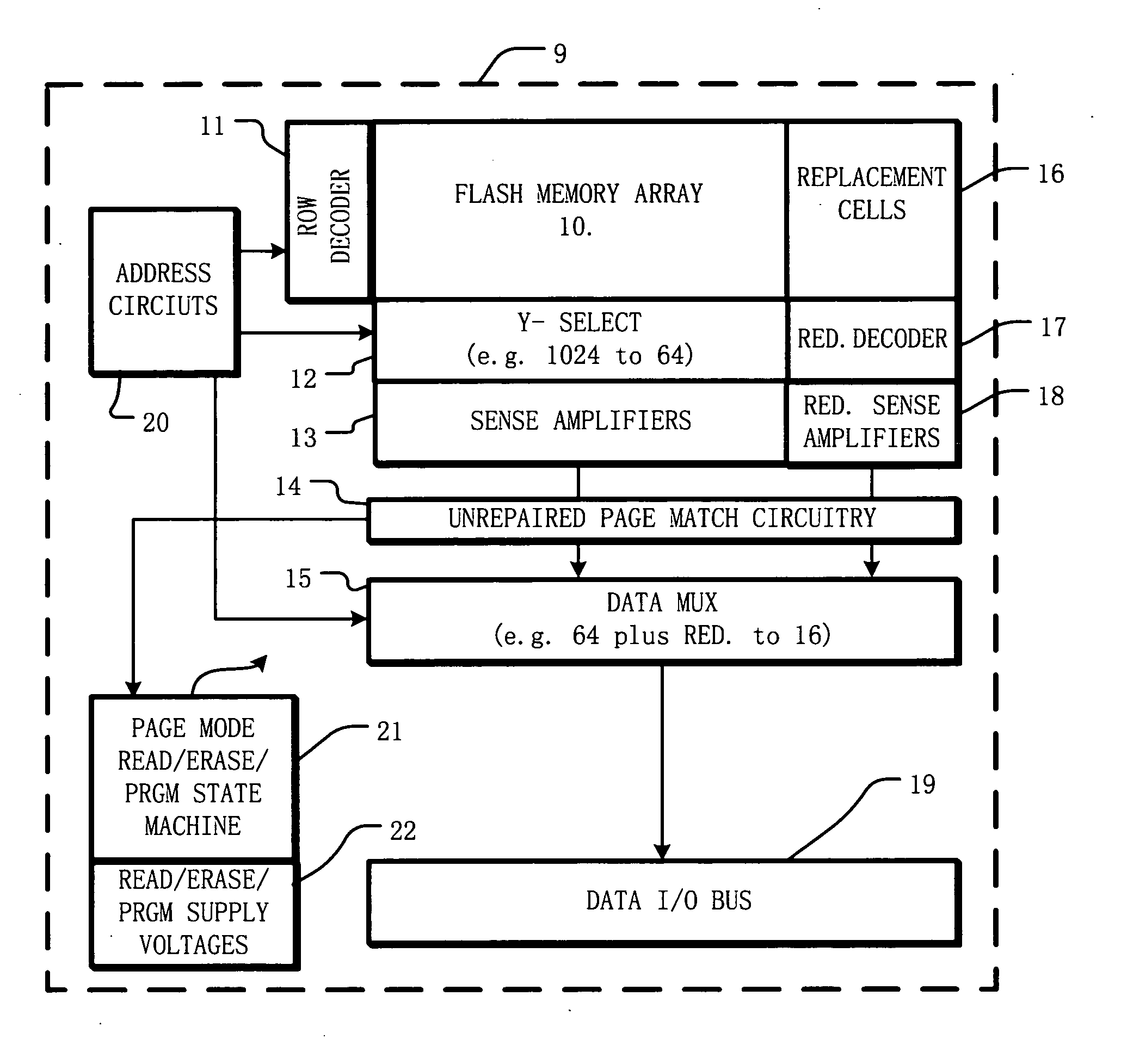
[0034] As used herein, the term “bit line” refers to a conductor extending along a column in the array used during access to memory cells along the column, while the term “data line” more generally refers to a bit line and other types of lines carrying data, such as lines on the outputs of sense amplifiers, column select lines and data multiplexers. Bit lines are defective when data sensed from memory cells using the bit line is unreliable. In typical memory devices including redundant arrays of replacement cells, bit lines are marked defective by storing addresses on the chip as indicators that identified bit lines are defective. Attempts to access memory cells using the defective bit lines are diverted to the redundant array in response to the stored addresses.

[0035]FIG. 1 is a simplified block diagram of a single chip, integrated circuit memory device 9 supporting m...


PUM


Abstract

A method for operating an integrated circuit memory device includes applying a verify procedure in which the page of data and one or more bits from a set of replacement cells are matched with a pattern in parallel to indicate a verify result, where the page of data is “unrepaired” and may include one or more bits from defective bit lines. While matching to indicate a verify result, the one or more bits from defective bit lines in the page are masked. Flash memory and other memory devices implement the method.

Description

RELATED APPLICATION [0001] The present application claims benefit of U.S. provisional application No. 60 / 579,359, filed on 14 Jun. 2004.BACKGROUND OF THE INVENTION [0002] 1. Field of the Invention [0003] The present invention relates generally to memory devices and more particularly to a nonvolatile memory device having a page read operation. [0004] 2. Description of Related Art [0005] Nonvolatile memory devices typically include a memory array comprising memory cells that maintain their data even when electrical power has been removed from the device. There are a variety of types of nonvolatile memory devices. One type includes so-called “read only memory,” like mask ROM in which the data is stored in the memory cell by implanting impurities in the channel region of MOS transistors. The data stored in mask ROM devices, and other nonvolatile read only memory devices, cannot be changed in the field. Another type of nonvolatile memory device includes electrically erasable and programm...

Claims


Application Information

Patent Timeline
IPC IPC(8): G11C7/00G11C7/10G11C29/00
CPCG11C7/1021G11C2216/14G11C29/846G11C29/82
Inventor MEIHONG, ZHUJING, WANGCHAO, YANG NIEN
Owner MACRONIX INT CO LTD
Learn More