Process for making light waveguide element

a technology of light waveguide and element, which is applied in the direction of optical waveguide light guide, instruments, optics, etc., can solve the problems of low production efficiency of conventional process, reduced yield, and difficulty in making etching stable, so as to minimize the variation of film thickness within the wafer, precise vertical optical axis alignment, and precise control of film thickness

Inactive Publication Date: 2005-12-15
NEOPHOTONICS CORP
View PDF4 Cites 0 Cited by
  • Summary
  • Abstract
  • Description
  • Claims
  • Application Information

AI Technical Summary

Benefits of technology

[0015] It is preferred that said T-shaped upper clad layer is made 15 μm thick or more to assure the required thickness for light propagation characteristics. The optical axis height-adjusting sections may made so as to have a thickness from said lower clad layer equal to the sum of a half of a thickness of said core and an optical axis height of said optical fiber and said photoelectric components to enable precise vertical optical axis alignment with the optical fiber and photoelectric components. The core and said upper clad layer may be made by plasma chemical vapor deposition to minimize variations in the film thickness within the wafer and enable precise control of the film thickness, thus maximizing the yield and providing precise optical axis height-adjusting sections.

Problems solved by technology

In such a conventional method, however, the etching rate depends on the etching depth and the reaction product adhered to the chamber so that it is difficult to make the etching stable.
Moreover, variations in the etching rate in the chamber or the wafer surface make it difficult to provide uniform etching between wafers or within the wafer surface, resulting in the reduced yield.
Thus conventional process has low productivity and fails to produce the light waveguide element economically.

Method used


Image

  • Process for making light waveguide element
  • Process for making light waveguide element
  • Process for making light waveguide element

Examples


second embodiment

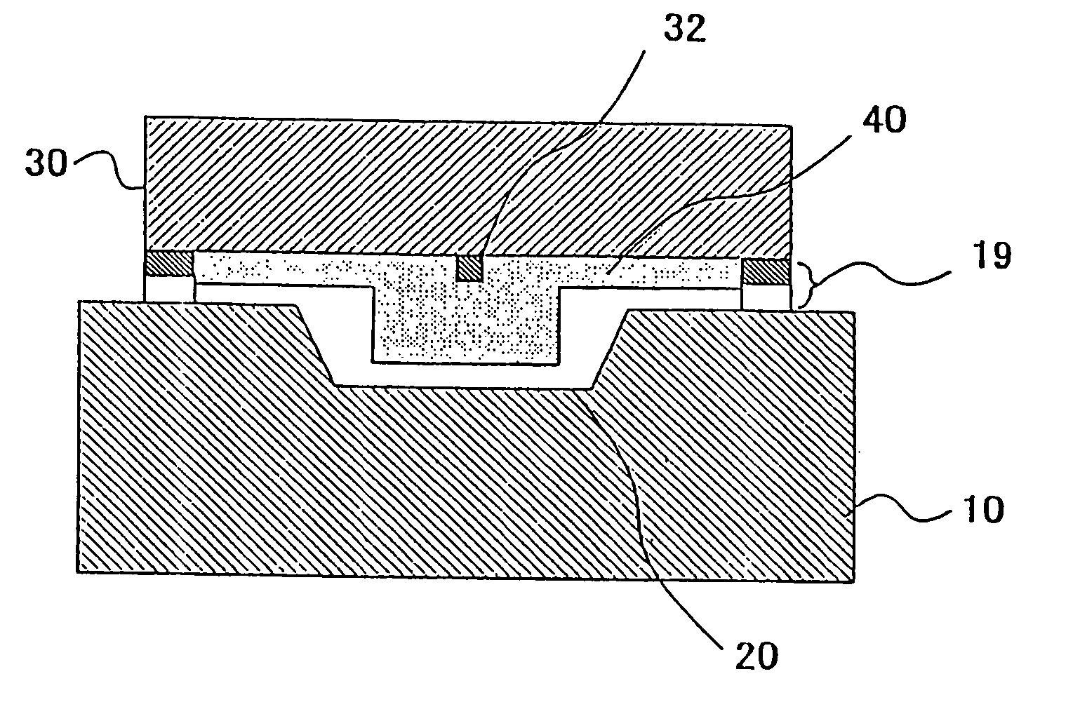
[0034] In FIG. 8(a), a core 32 and the first height-adjusting layer 33 are formed on the lower clad layer or substrate 30, and an etching stopper film 34 is formed on the first height-adjusting layer 33. The thickness of each of the core 32 and the first height-adjusting layer 33 is 5.0 μm. The etching stopper film 34 also works as a marker for matching the optical axis in the direction of a plane on which the light waveguide element is mounted.

[0035] In FIG. 8(b), the first upper clad layer or quartz film 36 having a thickness of 10 μm is formed and, then, an etching mask 38 is formed to cover the area above the core 32. Then, the portion of the first upper clad layer 36 other than the area covered by the etching mask 38 is etched off. It is continued until at least the etching stopper film 34 is exposed as shown in FIG. 8(c).

[0036] In FIG. 8(d), photolithography and etching are employed to remove the etching mask 38.

[0037] In FIG. 8(e), the second upper clad layer or quartz fil...

third embodiment

[0040] In FIG. 10(a), a core film 31 is formed on a lower clad layer or substrate 30, and an etching stopper film 34, which also serves as horizontal optical axis-matching markers, and a core pattern-forming etching mask 35 are formed on the core film 31. The thickness of the core film 31 is made 5.0 μm.

[0041] In FIG. 10(b), the first upper clad layer or quartz film 36 having a thickness of 6.5 μm is formed and, then, a marker-etching mask 37 is formed so as to cover the area above the etching stopper film 34. Then, the portion of the first upper clad layer 36 and the core film 31 other than the area covered by the marker-etching mask 37 are etched off. It is continued until at least the portion of the core film 31 is removed as shown in FIG. 10(c).

[0042] In FIG. 10(d), photolithography and etching are used to remove only the etching mask 35 from the core 32 and, then, the second upper clad layer or quartz film 40 having a thickness of 15 μm is formed.

[0043] In FIG. 10(e), an etc...


PUM


Abstract

A light waveguide element is made by forming only an upper clad layer (40) and a core layer (32) without etching an optical axis height-adjusting sections. By using plasma chemical vapor deposition (CVD) which is good at controlling the film thickness, it is possible to provide without difficulty a light waveguide element with a height-adjusting section that has a precise film thickness, making it possible to provide precise optical axis vertical alignment upon mounting. By forming alignment markers in the same photolithography as that of the core formation, it is possible to provide precise horizontal optical axis alignment.

Description

CROSS-REFERENCE TO RELATED APPLICATIONS [0001] This is a divisional application of prior application Ser. No. 10 / 238,652 filed Sep. 11, 2002, pending.BACKGROUND OF THE INVENTION [0002] 1. Field of the Invention [0003] The present invention relates to a process for making an economical light waveguide element mounted on a mount board along with an optical fiber and photoelectric components and enabling precise optical axis alignment. [0004] 2. Description of the Related Art [0005] Japanese patent application Kokai No. 10-133069 discloses a method of mounting a light waveguide element, by which the light waveguide element is mounted on the same silicon substrate along with the optical fiber and photoelectric components to which the light waveguide element is connected. It is mounted such that the upper surface of the light waveguide element layer faces the standard surface of the silicon substrate so that the thickness of the clad layer of the light waveguide element is adjusted to ma...

Claims


Application Information

Patent Timeline
Patent Type & Authority Applications(United States)
IPC IPC(8): G02B6/12G02B6/122G02B6/13G02B6/136G02B6/30G02B6/42
CPCG02B6/136G02B6/30G02B6/42G02B2006/12176G02B6/4224G02B6/4228G02B6/4201G02B6/424G02B6/4245G02B6/4261
Inventor UNO, YUTAKA
Owner NEOPHOTONICS CORP
Why Eureka
Try Eureka