Multipiece apparatus for thermal and electromagnetic interference (EMI) shielding enhancement in die-up array packages and method of making the same

a technology of electromagnetic interference and die-up array, which is applied in the direction of electrical apparatus, semiconductor devices, semiconductor/solid-state device details, etc., can solve the problems of poor thermal performance, inadequate emi protection, and heat generated by the ic die trapped in the bga package, and achieve the effect of enhancing thermal performance and electromagnetic interference (emi) shielding

Active Publication Date: 2005-12-22
AVAGO TECH INT SALES PTE LTD
View PDF99 Cites 126 Cited by
  • Summary
  • Abstract
  • Description
  • Claims
  • Application Information

AI Technical Summary

Problems solved by technology

Problems with conventional BGA packages include poor thermal performance and inadequate EMI protection.
When materials with poor thermal conductivity surround the IC die, heat generated by the IC die is trapped within the BGA package.
Consequently, EMI generated by the IC die can pass through the resin substrate and plastic molding compound and interfere with electronic components outside of the package.
Likewise, EMI generated by electronic components outside of the package can pass through the resin substrate and plastic molding compound and interfere with the IC die.

Method used


Image

  • Multipiece apparatus for thermal and electromagnetic interference (EMI) shielding enhancement in die-up array packages and method of making the same
  • Multipiece apparatus for thermal and electromagnetic interference (EMI) shielding enhancement in die-up array packages and method of making the same
  • Multipiece apparatus for thermal and electromagnetic interference (EMI) shielding enhancement in die-up array packages and method of making the same

Examples


Embodiment Construction

Overview

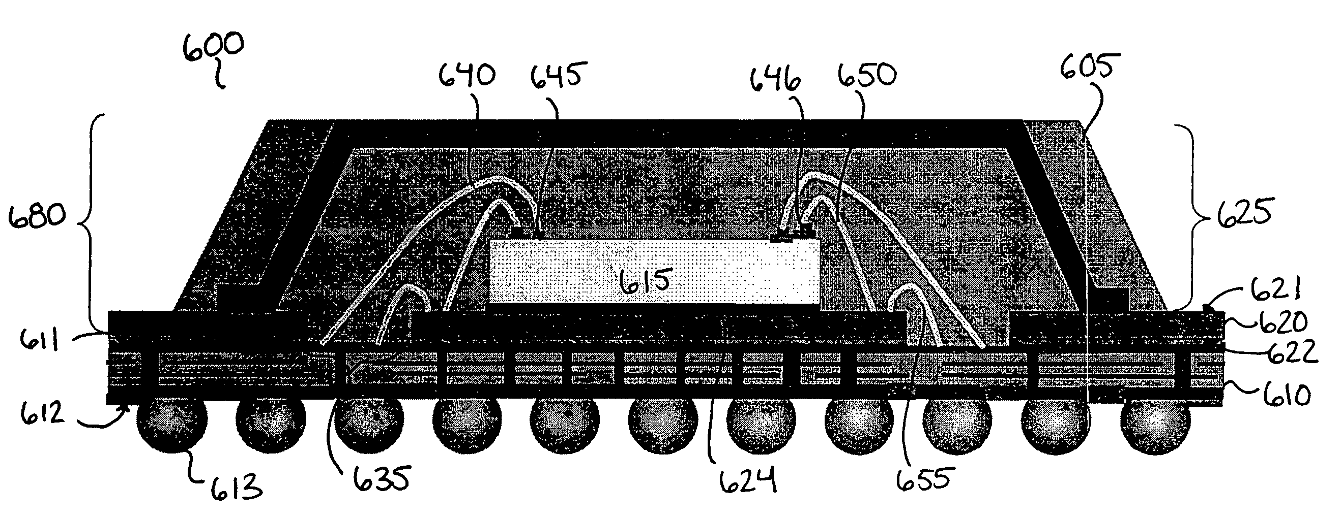
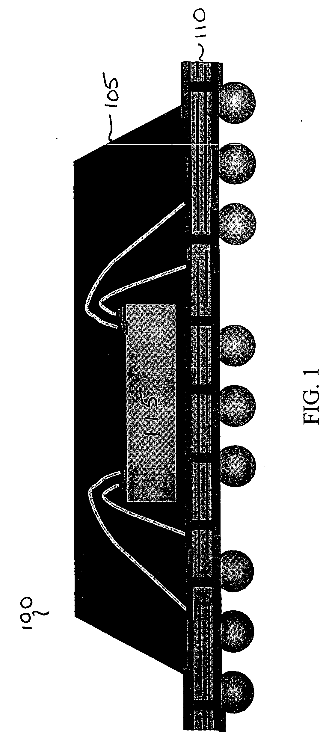
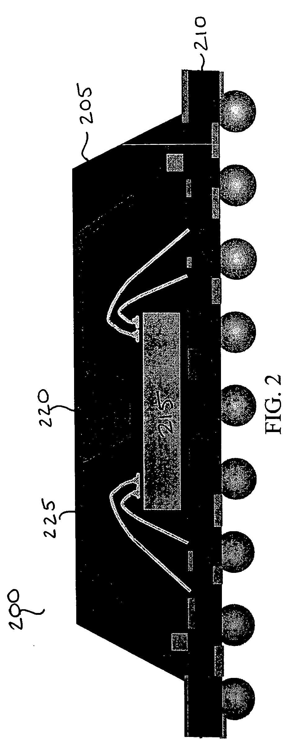
[0051] The present invention is directed to an apparatus and method for enhancing thermal performance and electromagnetic interference (EMI) shielding in die-up array integrated circuit (IC) device packages. A die-up array IC device package includes a plurality of electrically conductive terminals (e.g., solder balls, pins, pads, etc.) arranged in an array (e.g., columns and rows) on a bottom surface of a substrate. Signals from an IC die mounted on a top surface of the substrate are routed through the substrate to the electrically conductive terminals. The electrically conductive terminals are configured to be attached to a printed circuit board (PCB). Examples of die-up array packages include BGA (e.g., pad array carrier, pad array package, land grid array, pad grid array packages), pin grid array, etc.

[0052] In embodiments of the present invention, a die-up array-type IC device package includes an IC die mounted to a first surface of a stiffener, and a package substrat...


PUM


Abstract

A die-up array integrated circuit (IC) device package and method of making the same is presented. A frame body has opposing first and second surfaces and a central opening that is open at the first and second surfaces. The second frame body surface is mounted to a first stiffener surface. An IC die is mounted to the first stiffener surface within the central opening through the frame body. A planar lid has opposing first and second surfaces. The second lid surface is coupled to the first frame body surface. A first substrate surface is coupled to a second stiffener surface. An array of electrically conductive terminals is coupled to a second substrate surface. The stiffener, frame body, and lid form an enclosure structure substantially enclosing the IC die. The die enclosure spreads heat from the IC die, and shields EMI emanating from and radiating toward the IC die.

Description

CROSS-REFERENCE TO RELATED APPLICATIONS [0001] The following patent application of common assignee is related to the present application, and is herein incorporated by reference in its entirety: “Ball Grid Array Package Enhanced With A Thermal And Electrical Connector,” U.S. patent application Ser. No. 10 / 284,312, filed Oct. 31, 2002. [0002] The following application of common assignee is related to the present application, has the same filing date as the present application, and is herein incorporated by reference in its entirety: “Apparatus And Method For Thermal And Electromagnetic Interference (EMI) Shielding Enhancement In Die-Up Array Packages,” Atty. Dkt. No. 1875.5480000, Ser. No. ______.BACKGROUND OF THE INVENTION [0003] 1. Field of the Invention [0004] The invention relates generally to the field of integrated circuit (IC) device packaging technology and, more particularly to thermal enhancement and electromagnetic interference (EMI) shielding in IC device packages. [0005]...

Claims


Application Information

Patent Timeline
Patent Type & Authority Applications(United States)
IPC IPC(8): H01L21/44H01L23/12H01L23/24H01L23/31H01L23/433H01L23/552
CPCH01L23/24H01L2224/32225H01L23/4334H01L23/552H01L24/49H01L2224/48091H01L2224/48227H01L2224/48228H01L2224/48237H01L2224/48465H01L2224/4911H01L2924/01006H01L2924/01013H01L2924/01028H01L2924/01029H01L2924/01047H01L2924/0105H01L2924/01074H01L2924/01078H01L2924/01079H01L2924/01082H01L2924/09701H01L2924/14H01L2924/15311H01L2924/16151H01L2924/16152H01L2924/19107H01L2924/3011H01L2924/3025H01L23/3128H01L2224/73265H01L2924/014H01L24/48H01L2924/01033H01L2924/00014H01L2924/00012H01L2924/00H01L2924/181H01L24/73H01L2224/45099H01L2224/05599
Inventor ZHAO, SAM Z.KHAN, REZA-UR R.
Owner AVAGO TECH INT SALES PTE LTD
Why Eureka
Try Eureka