Method and system for inspecting a wafer

a wafer and inspection method technology, applied in the direction of measuring devices, material analysis through optical means, instruments, etc., can solve the problem of general inability to measure the test item exactly the same position, and achieve the effect of sufficient contras

Inactive Publication Date: 2005-12-22
VISTEC SEMICON SYST
View PDF9 Cites 49 Cited by
  • Summary
  • Abstract
  • Description
  • Claims
  • Application Information

AI Technical Summary

Benefits of technology

[0011] An object of the present invention is therefore to provide a method and a system for inspecting wafers, in particular for detecting

Problems solved by technology

In automated non-contact measurement, it is generally impossible t

Method used


Image

  • Method and system for inspecting a wafer
  • Method and system for inspecting a wafer
  • Method and system for inspecting a wafer

Examples


Embodiment Construction

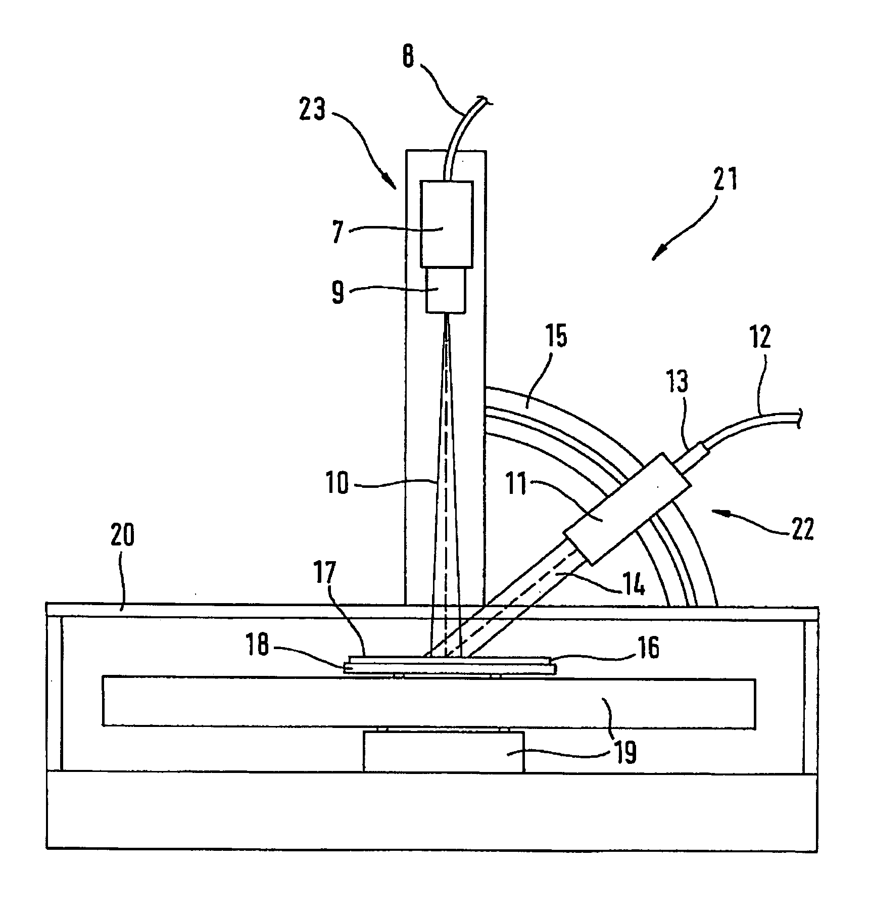
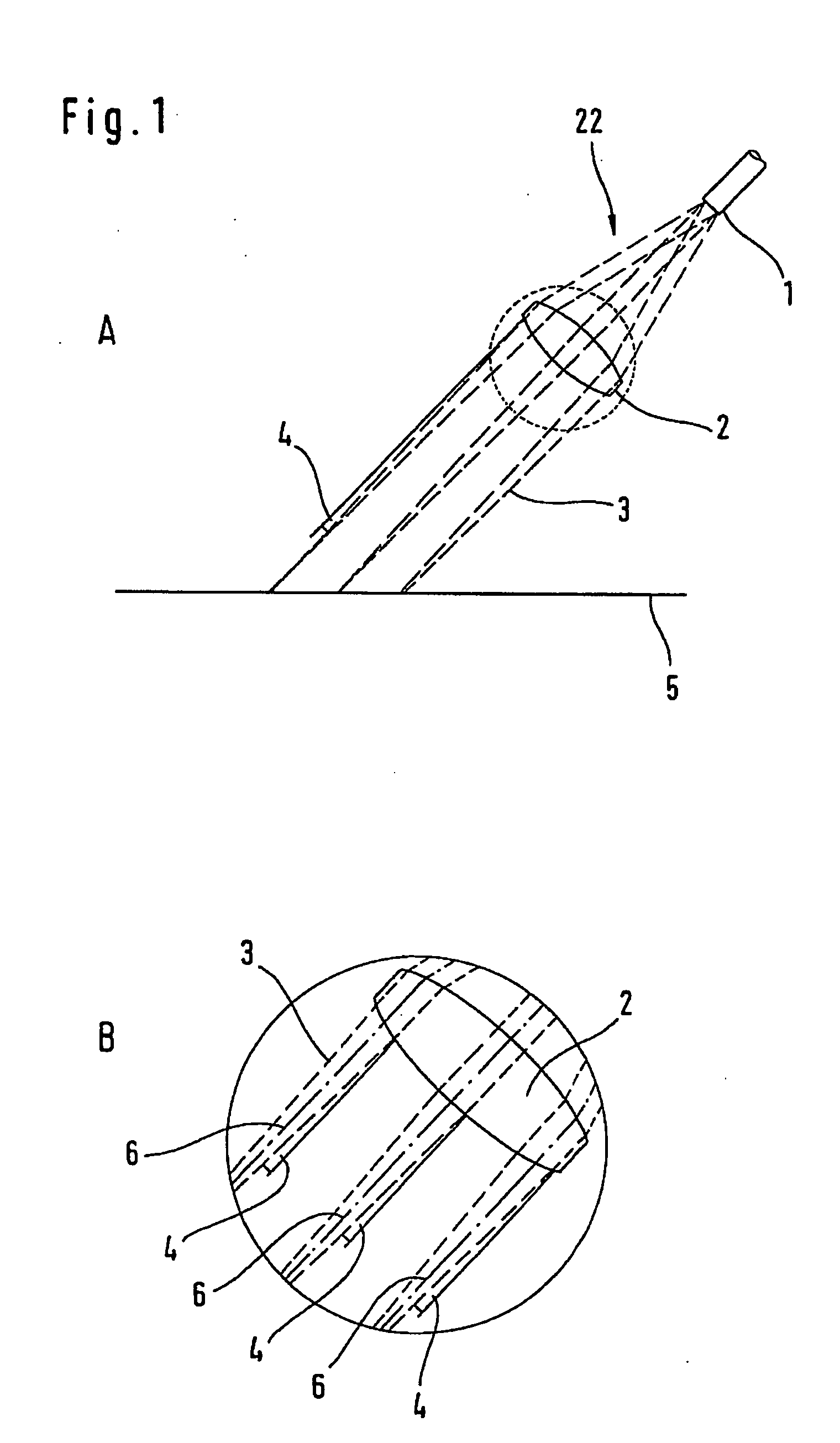
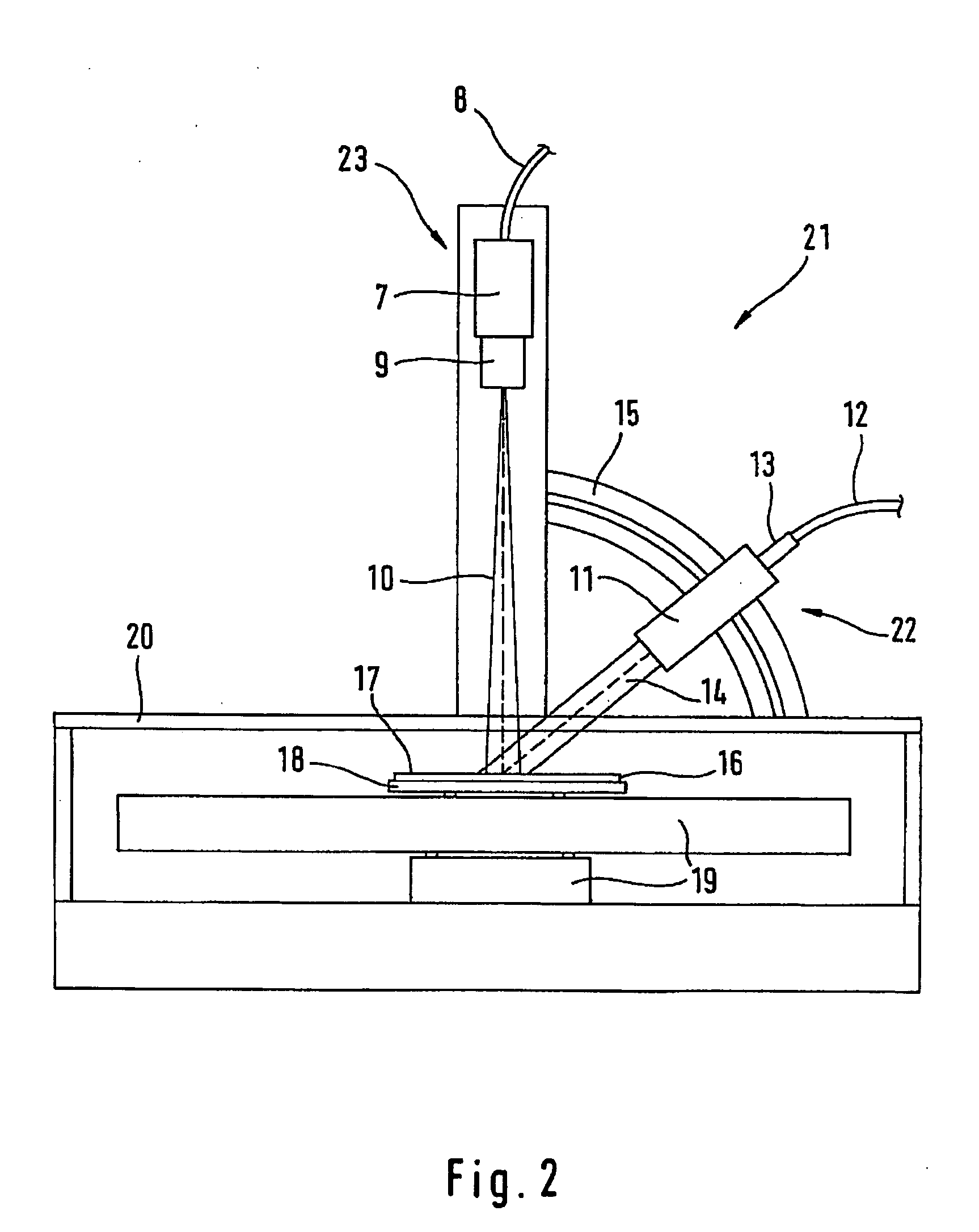
[0041]FIG. 1 shows the basic principle of the telecentric illumination, according to the present invention, of an object plane 5 which, in the concrete application, represents a wafer surface. A small-area planar radiator, as represented by an optical waveguide, is used as radiation source 22 in this exemplifying embodiment. Beam bundles 3 extending in parallel fashion and having a small illumination aperture 4 are generated by means of a lens system 2 (collimating optical system), depicted here only schematically. Beam bundles 3 strike object plane 5 in such a way that every point on that object plane is illuminated from the same spatial direction and at the same solid angle.

[0042] The region outlined with a dotted circle in FIG. 1A is reproduced in enlarged fashion in FIG. 1B. The beam bundles extending in parallel fashion are once again labeled 3. It is clearly evident from the detail view that axes 6 of beam bundles 3 extend parallel to one another. Illumination aperture 4 in t...


PUM


Abstract

A method for inspecting a wafer includes telecentrically illuminating, with a radiation source, a region of the wafer surface to be inspected. An image of wafer region is acquired using a camera. The wafer region is inspected using the acquired image.

Description

CROSS REFERENCE TO RELATED APPLICATIONS [0001] Priority is claimed to German patent application 10 2004 029 014.8, the entire disclosure of which is hereby incorporated by reference herein. FIELD OF THE INVENTION [0002] The invention concerns a method for inspecting a wafer, in particular for detecting macrodefects such as exposure defects, at least one region to be inspected of the wafer surface being illuminated with a radiation source, an image of that surface region being acquired by means of a camera, and the wafer surface being inspected on the basis of the image obtained; as well as a wafer inspection system having a radiation source for illuminating at least one region to be inspected of the wafer surface, and having a camera for acquiring an image of that surface region. BACKGROUND OF THE INVENTION [0003] Inspection of wafers having an exposed resist layer is used for defect detection in semiconductor fabrication. During the process of exposing a wafer coated with resist, s...

Claims


Application Information

Patent Timeline
IPC IPC(8): G01N21/88G01N21/95G01N21/956
CPCG01N21/956G01N21/9501
Inventor BACKHAUSS, HENNINGKREH, ALBERT
Owner VISTEC SEMICON SYST
Why Eureka
Try Eureka