Method of driving data lines, and display device and liquid crystal display device using method

Active Publication Date: 2005-12-22
SHARP KK
View PDF5 Cites 9 Cited by
  • Summary
  • Abstract
  • Description
  • Claims
  • Application Information

AI Technical Summary

Benefits of technology

[0034] The objective of the present invention is to provide a method of driving a liquid crystal display device, by which a striped pattern on a reproduced image is restrained to be i

Problems solved by technology

Therefore, this method causes the striped pattern on account of the voltage variations to be unnoticeable.
In other words, since the voltage variations on the respective signal l

Method used


Image

  • Method of driving data lines, and display device and liquid crystal display device using method
  • Method of driving data lines, and display device and liquid crystal display device using method
  • Method of driving data lines, and display device and liquid crystal display device using method

Examples


embodiment 1

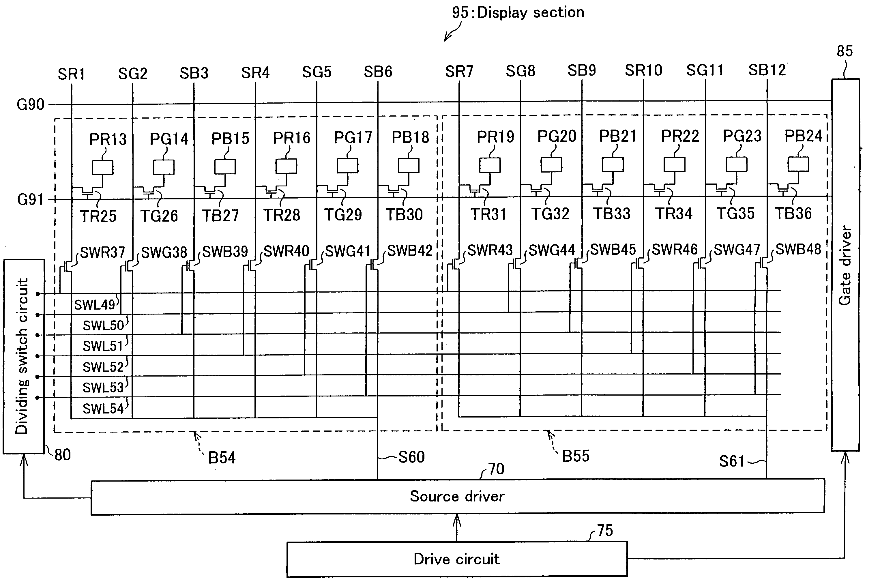
[0073] An embodiment of the present invention is described below in reference to FIGS. 1 and 2.

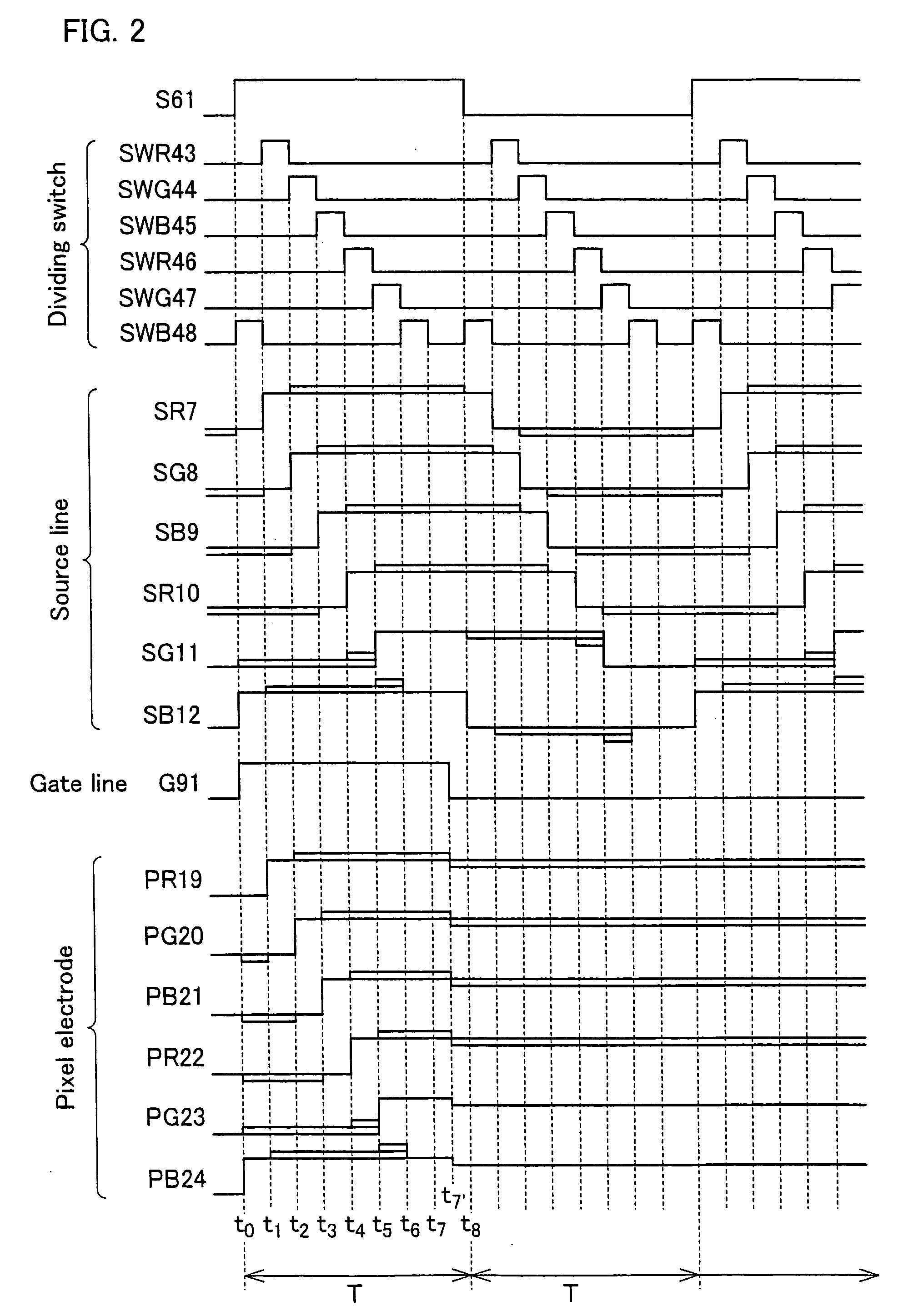
[0074]FIG. 2 is a timing chart regarding the block B55 on the occasion of displaying a uniform color, e.g. a halftone, on the whole screen. In the figure, one horizontal period (period for scanning one gate line) is referred to as T. It is also noted that the figure relates to three horizontal periods (periods for scanning three gate lines including the gate lines G90 and G91).

[0075] During the period T, the signal voltage S61 is supplied from the source driver 70 to six source lines SR7 through SB12 of the block B55. With this, the signal voltage S61 is written into the pixel electrodes (PR19 through PB24) of the block B55. Also, in synchronism with the aforesaid writing of the signal voltage S61, the signal voltage S60 is written into the pixel electrodes (PR13 through PB18) of the block B54. As a result, during the period T, the signal voltages (e.g. S60 and S61) supplied from the sou...

embodiment 2

[0102] The following will describe another embodiment of the present invention in reference to FIGS. 1 and 3. Note that, a display section of the present embodiment is basically identical with that of Embodiment 1, except that, in the present embodiment, (i) the timings of controlling the dividing switches by the dividing switch circuit and (ii) the timings at which the source driver applies signal voltages to the output signal lines are different from the timings in Embodiment 1. On this account, members of the display section, having the same functions as those described in Embodiment 1, are given the same numbers, so that the descriptions are omitted for the sake of convenience.

[0103]FIG. 3 is a timing chart regarding the block B55 (see FIG. 1) on the occasion of displaying a uniform color, e.g. a halftone, on the whole screen. In the figure, one horizontal period (period for scanning one gate line) is referred to as T. It is also noted that the figure relates to three horizonta...


PUM


Abstract

A method of driving source lines is arranged as follows: One output signal line S61 of a source driver is connected to a plurality of lines corresponding to respective source lines SR7 through SB12, and these source lines from SR7 (starting data line) to SB12 (terminating data line) are grouped as one block (group). In each block, a signal voltage of a divided output is supplied to the source lines during a first horizontal period T, while a signal voltage whose polarity is opposite to that of the aforesaid output is supplied to the source lines in a second horizontal period that is after the first horizontal period. In each of the horizontal periods, the source lines SR7 through SB12 are subjected to sequential selection. In addition to this, the source line SB12 is selected before turning the source line SR7 off. With this, a method of driving source lines, which can restrain (eliminate) the voltage variation on each source line and pixel electrode on account parasitic capacities between source lines, can be realized.

Description

[0001] This Nonprovisional application claims priority under 35 U.S.C. § 119(a) on Patent Application No. 2003-384183 filed in Japan on Nov. 13, 2003, the entire contents of which are hereby incorporated by reference. FIELD OF THE INVENTION [0002] The present invention relates to a method of driving data lines, and particularly to a method of driving source lines of a liquid crystal display device. BACKGROUND OF THE INVENTION [0003]FIG. 5 is a block diagram showing a liquid crystal display device in which a plurality of source lines are driven by dividing, using switches, one output (signal voltage) from a source driver. [0004] As in the figure, on the surface of a display section 195 of the liquid crystal display device, a plurality of gate lines G190, G191, . . . provided in crosswise and a plurality of source lines SR101, . . . , SB112, . . . provided in lengthwise are laid out in a matrix manner. For instance, at the respective intersections of the gate line G191 and the source ...

Claims


Application Information

Patent Timeline
IPC IPC(8): G02F1/133G09G3/20G09G3/36G11C8/00
CPCG09G3/3614G09G3/3685G09G2320/0219G09G2310/06G09G2310/0297G09G3/36
Inventor OKUNO, HARUMIYAMADA, JUNICHINAGATA, HISASHI
Owner SHARP KK
Why Eureka
Try Eureka