Semiconductor device and method of manufacturing the same

a technology of semiconductor devices and semiconductor films, which is applied in the direction of semiconductor devices, basic electric elements, electrical appliances, etc., can solve the problems of limited circuit design of semiconductor devices, complicated manufacturing processes, and thin thermal oxide films, so as to improve design freedom, facilitate manufacturing, and prevent the effect of increasing gate capacitan

Inactive Publication Date: 2009-06-11
LONGITUDE SEMICON S A R L
View PDF5 Cites 42 Cited by
  • Summary
  • Abstract
  • Description
  • Claims
  • Application Information

AI Technical Summary

Benefits of technology

[0013]According to the present invention, a semiconductor device including transistors of different channel lengths can easily be manufactured. Thereby, design freedom can be improved and an increase in gate capacitance can be prevented.

Problems solved by technology

Therefore, a circuit design of the semiconductor device is restricted in some cases.
However, multiple semiconductor layers are included in the above structure, complicating manufacturing processes.
Further, the thermal oxide film is so thin that insulation (isolation) is not sufficient.
As a result, the gate capacitance stored in the second p-type silicon semiconductor layer and the third n-type silicon semiconductor layer increases, making current-voltage characteristics unstable in some cases.
Further, recent semiconductor devices require high density and low power consumption.
However, a microscopic wiring or a contact arrangement design for high density and low power consumption cannot be performed in the structures disclosed in the above related arts.

Method used


Image

  • Semiconductor device and method of manufacturing the same
  • Semiconductor device and method of manufacturing the same
  • Semiconductor device and method of manufacturing the same

Examples


first embodiment

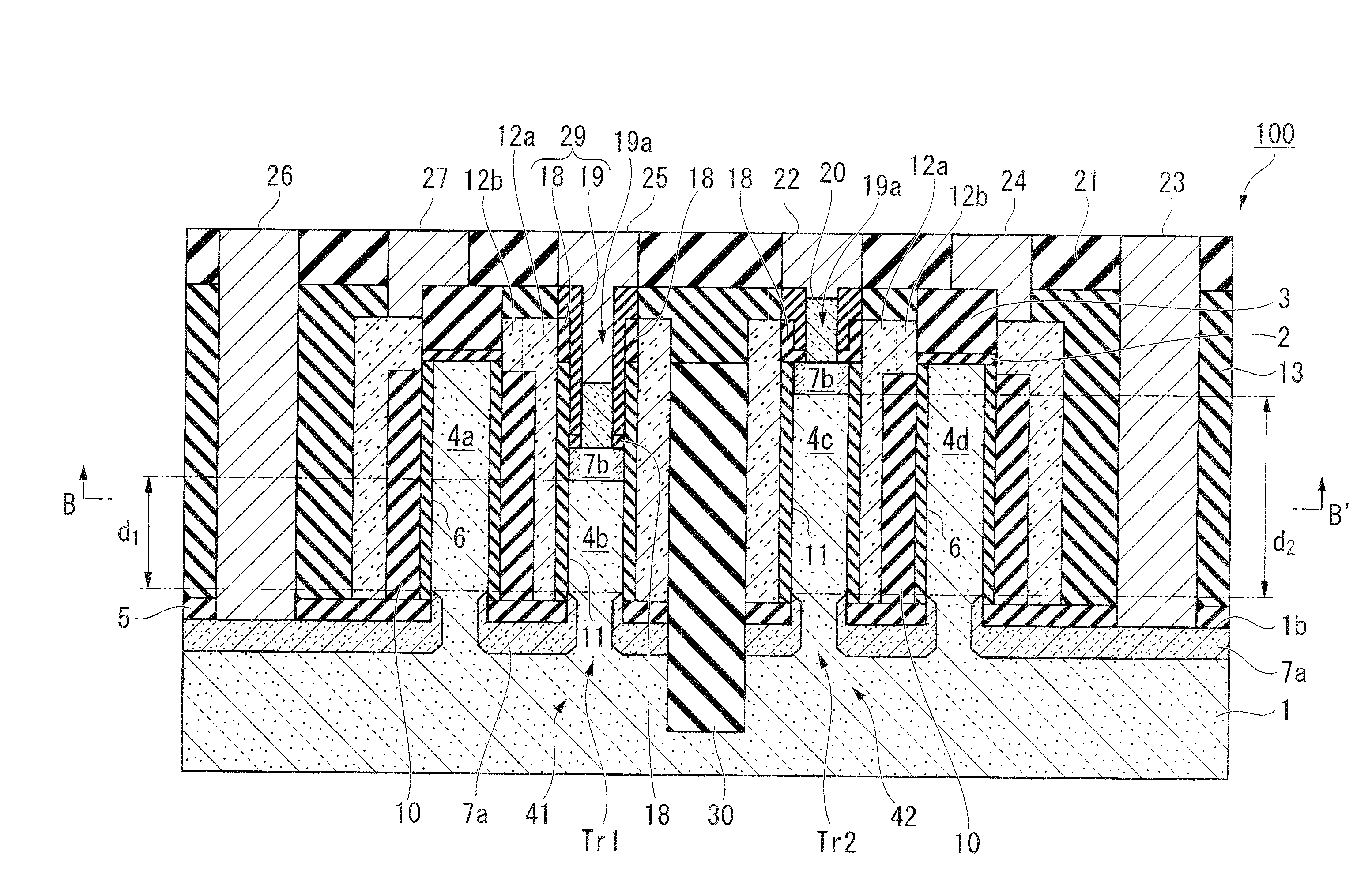
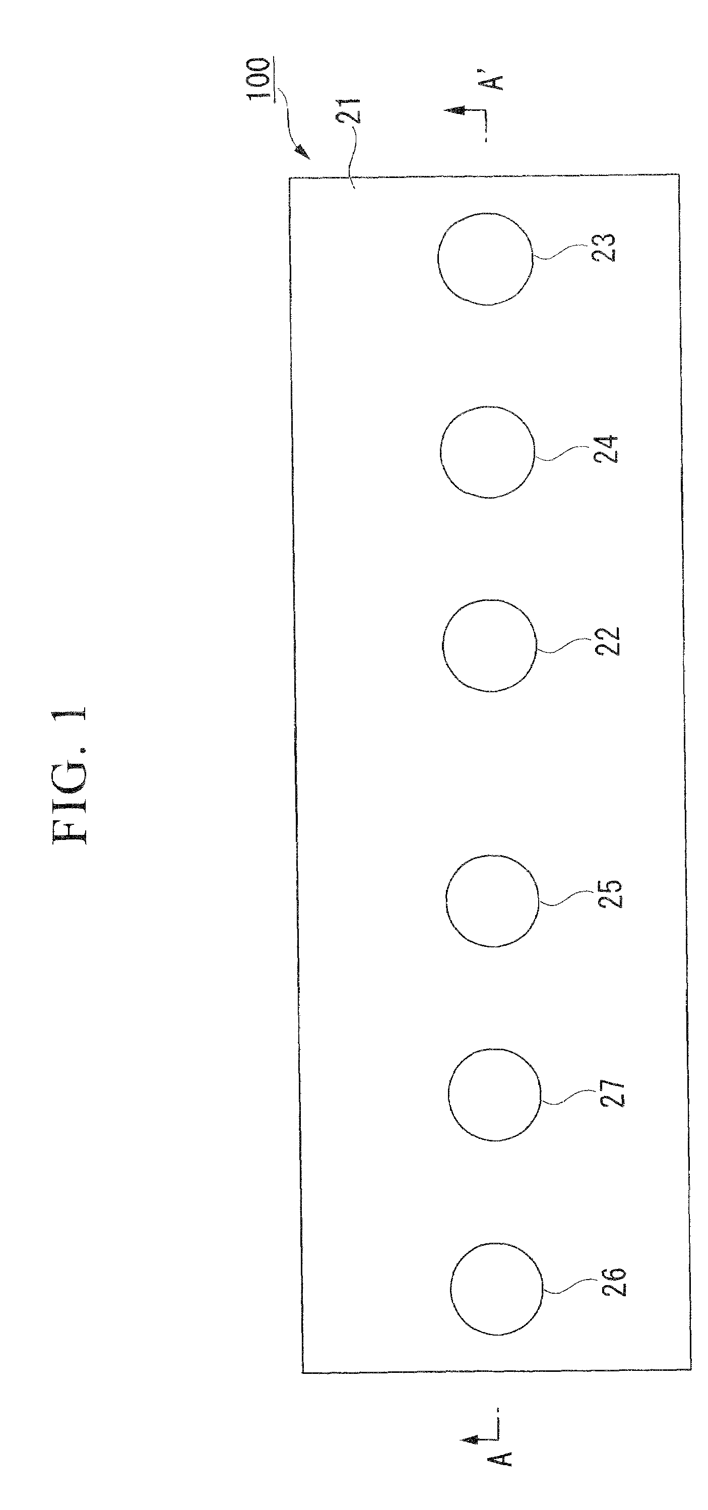
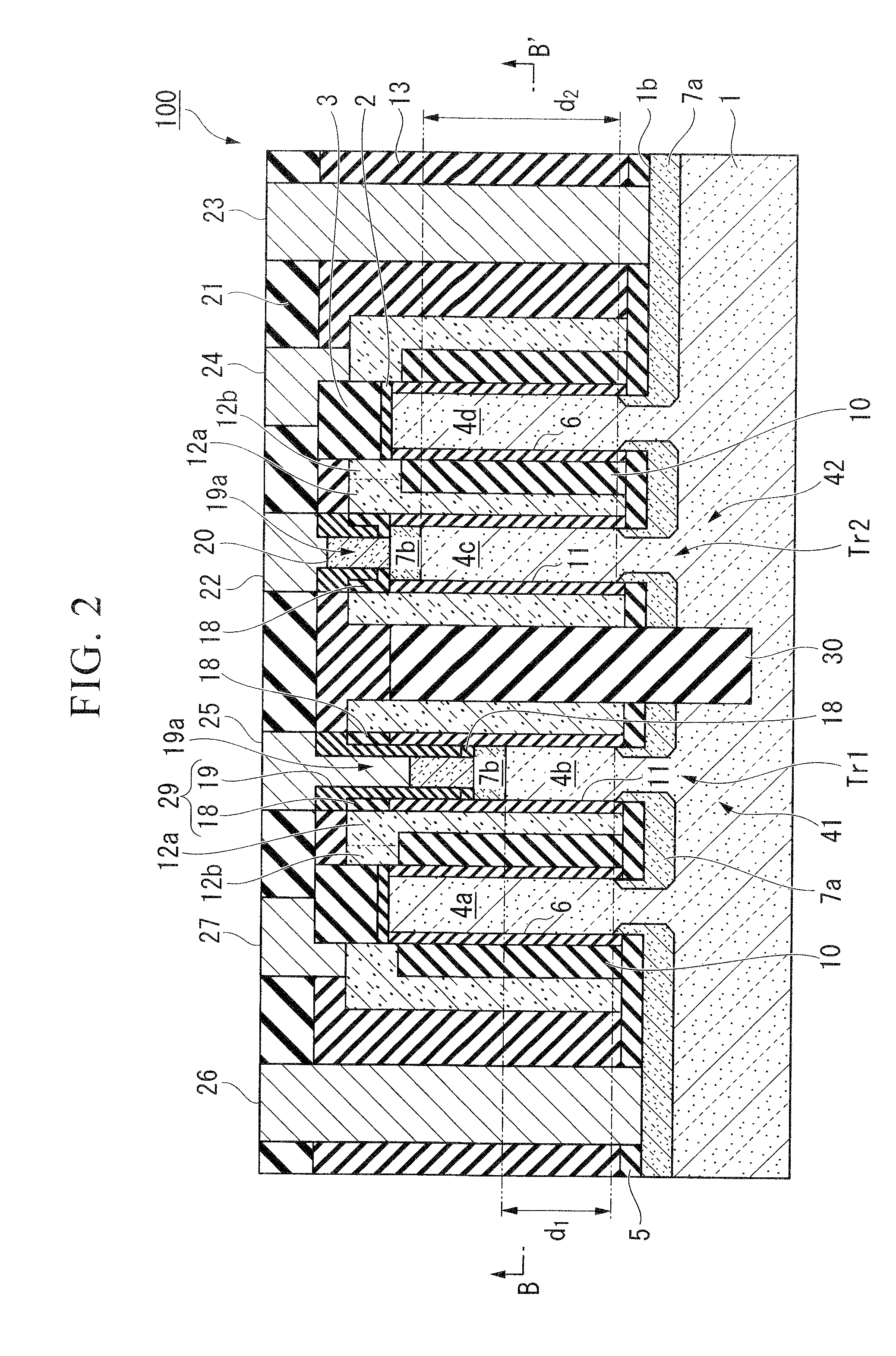
[0019]FIGS. 1 to 3 show an example of a semiconductor device according to a first embodiment of the present invention. FIG. 1 is a plane view, FIG. 2 is a cross-sectional view taken along an A-A′ line shown in FIG. 1, and FIG. 3 is a cross-sectional view taken along a B-B′ line shown in FIG. 2.

[0020]As shown in FIG. 1, circular contact-plug electrodes 22 to 27 arranged in series on a second inter-layer insulating film 21 are exposed when a semiconductor device 100 according to the first embodiment of the present invention is planarly viewed. The contact plug electrodes 22 to 27 are electrodes that supply current to sources, drains, and gates of vertical MOS transistors Tr1 and Tr2.

[0021]FIG. 2 is the cross-sectional view taken along the A-A′ line shown in FIG. 1.

[0022]The semiconductor device 100 has a structure in which the vertical MOS transistors Tr1 and Tr2 are formed in first-conductive-type active regions 41 and 42 isolated from each other by a shallow-trench isolation region ...

second embodiment

[0081]FIG. 22 is a cross-sectional view showing a semiconductor device according to a second embodiment of the present invention. Like reference numerals represent like elements of the first embodiment.

[0082]In a semiconductor device 101 according to the second embodiment, first semiconductor regions 7a of the second conductive type that are to be a source and a drain are formed on the bottom end of a channel silicon pillar 4f serving as a channel in the first-conductive-type active region 43 formed by the shallow-trench isolation region 30 formed on the semiconductor substrate 1 dividing the semiconductor substrate 1. The second semiconductor region 7b of the second conductive type is formed on the top end of the channel silicon pillar 4f. The gate insulating film 11 is formed to surround the channel silicon pillar 4f. The gate insulating film 11 is surrounded by the gate electrode 12a. Thus, the vertical MOS transistor Tr3 is formed.

[0083]A source-drain-voltage-supply silicon pill...


PUM


Abstract

A semiconductor device includes: a semiconductor substrate; multiple active regions of a first conductive type isolated from one another by shallow-trench isolation regions provided on one surface of the semiconductor substrate; multiple silicon pillars including channel silicon pillars formed in the active regions; multiple first semiconductor regions of a second conductive type that are respectively formed on bottom ends of the silicon pillars and to be sources or drains; multiple second semiconductor regions of the second conductive type that are formed on top ends of the silicon pillars and to be sources or drains; multiple gate insulating films surrounding the silicon pillars; and multiple gate electrodes surrounding the gate insulating films. At least one of the channel silicon pillars has a height different from that of another one of the channel silicon pillars.

Description

BACKGROUND OF THE INVENTION[0001]1. Field of the Invention[0002]The present invention relates to a semiconductor device and a method of manufacturing the same, and particularly to a semiconductor device including vertical MOS transistors of different channel lengths.[0003]Priority is claimed on Japanese Patent Application No. 2007-315747, filed Dec. 6, 2007, the content of which is incorporated herein by reference.[0004]2. Description of the Related Art[0005]As shown in FIG. 2 of US Patent Application Publication No. 2004 / 0262681 A1, a conventional three-dimensional transistor, i.e., a vertical MOS transistor, includes a silicon pillar to be a channel between source-drain diffusion layers. The channel portion of the silicon pillar is surrounded by a gate insulating film and a gate electrode. The source-drain diffusion layers are formed on the silicon pillar so as to completely cover the channel portion.[0006]In the vertical MOS transistor, an arrangement of vertical MOS transistors ...

Claims


Application Information

Patent Timeline
Patent Type & Authority Applications(United States)
IPC IPC(8): H01L21/336H01L21/3205
CPCH01L21/823412H01L29/7827H01L29/66666H01L21/823487
Inventor OYU, KIYONORI
Owner LONGITUDE SEMICON S A R L
Why Eureka
Try Eureka