
Image forming device for performing calibration by patch pattern

a technology of patch pattern and forming device, which is applied in the direction of optics, electrographic process apparatus, instruments, etc., can solve the problems of long time required for calibration step, and large amount of developer wasted in forming patch pattern, etc., and achieve the effect of simplifying the calibration step by patch pattern

Inactive Publication Date: 2005-12-22
SEIKO EPSON CORP
View PDF4 Cites 7 Cited by
  • Summary
  • Abstract
  • Description
  • Claims
  • Application Information

AI Technical Summary

Benefits of technology

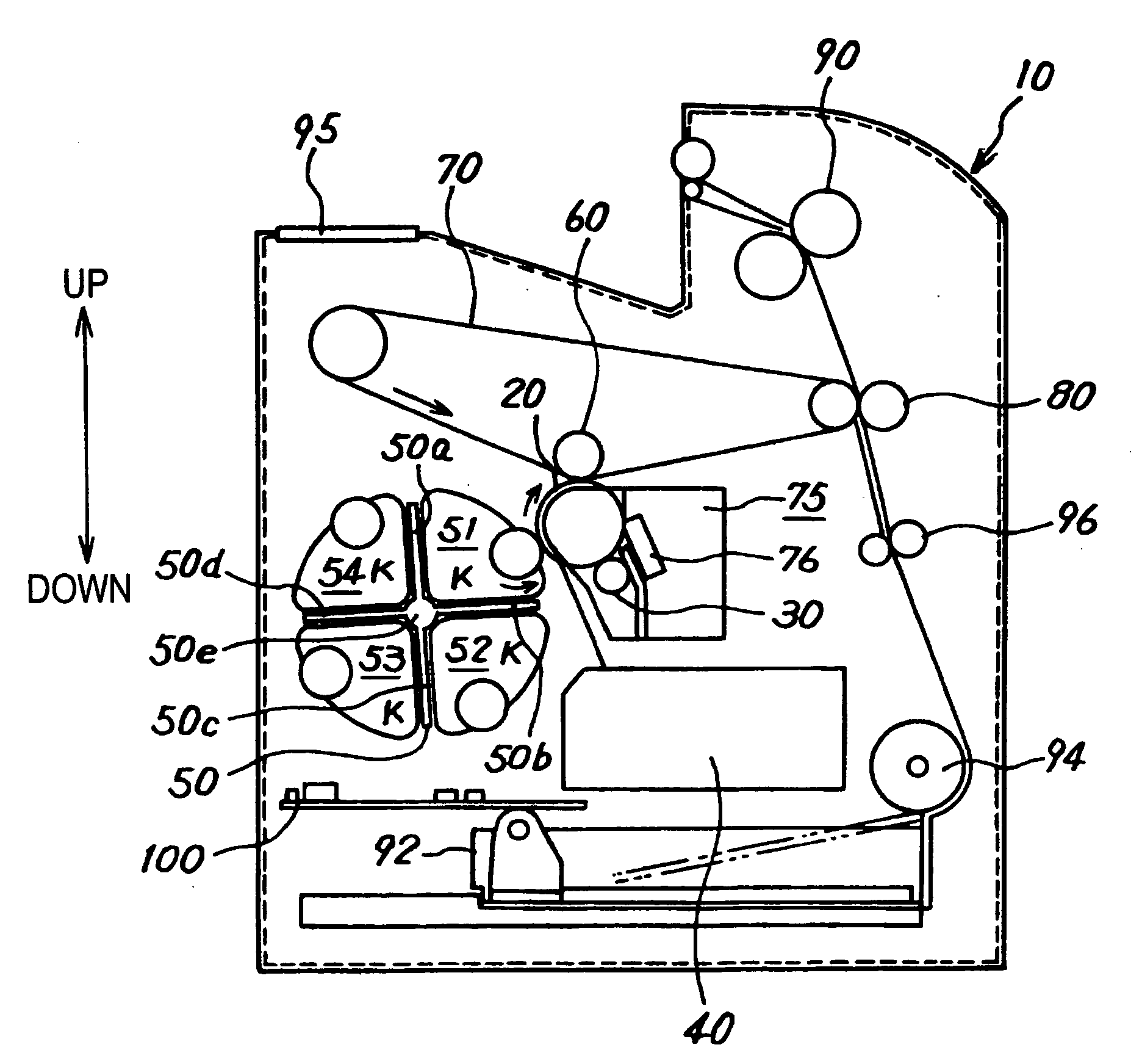
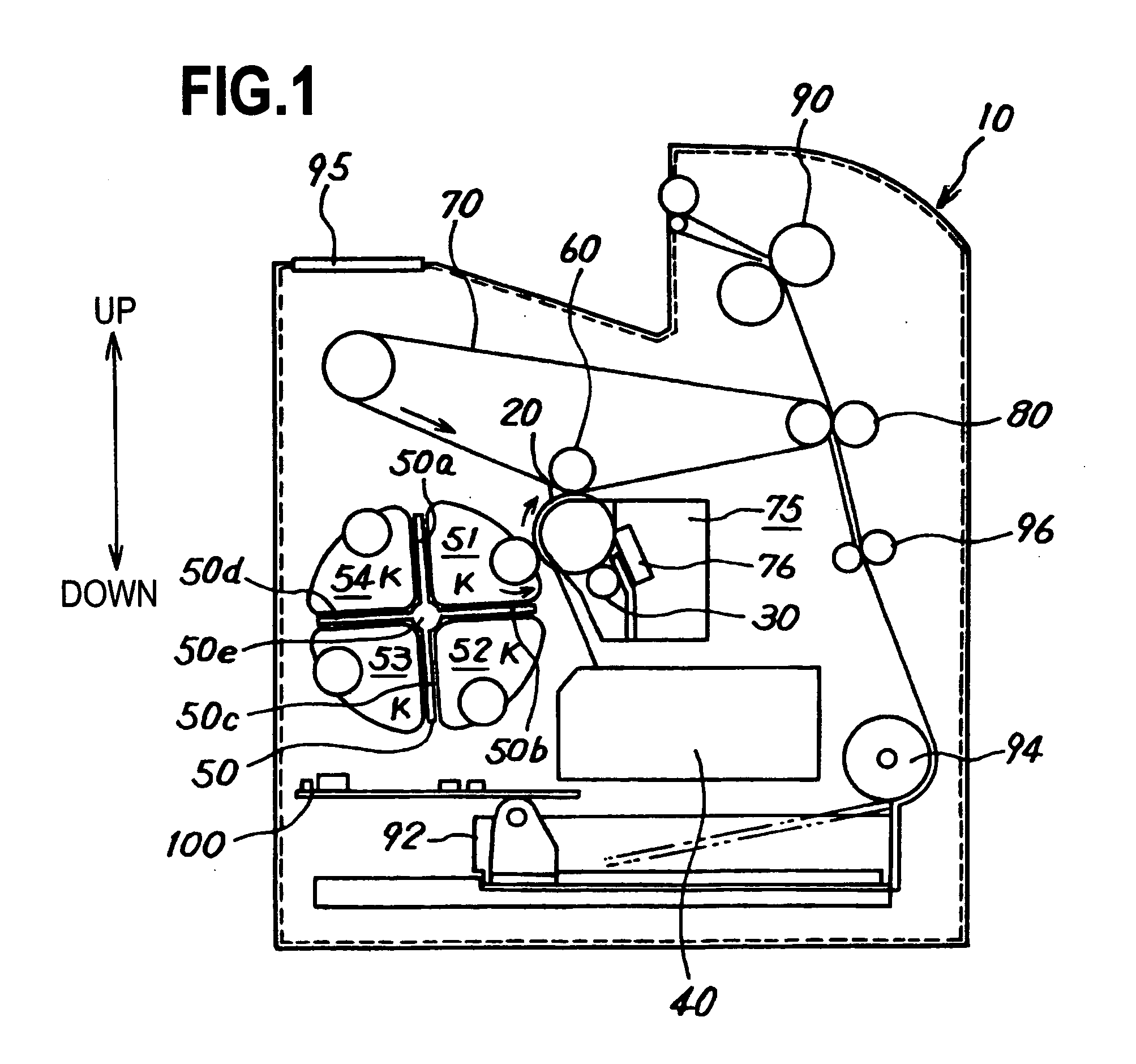
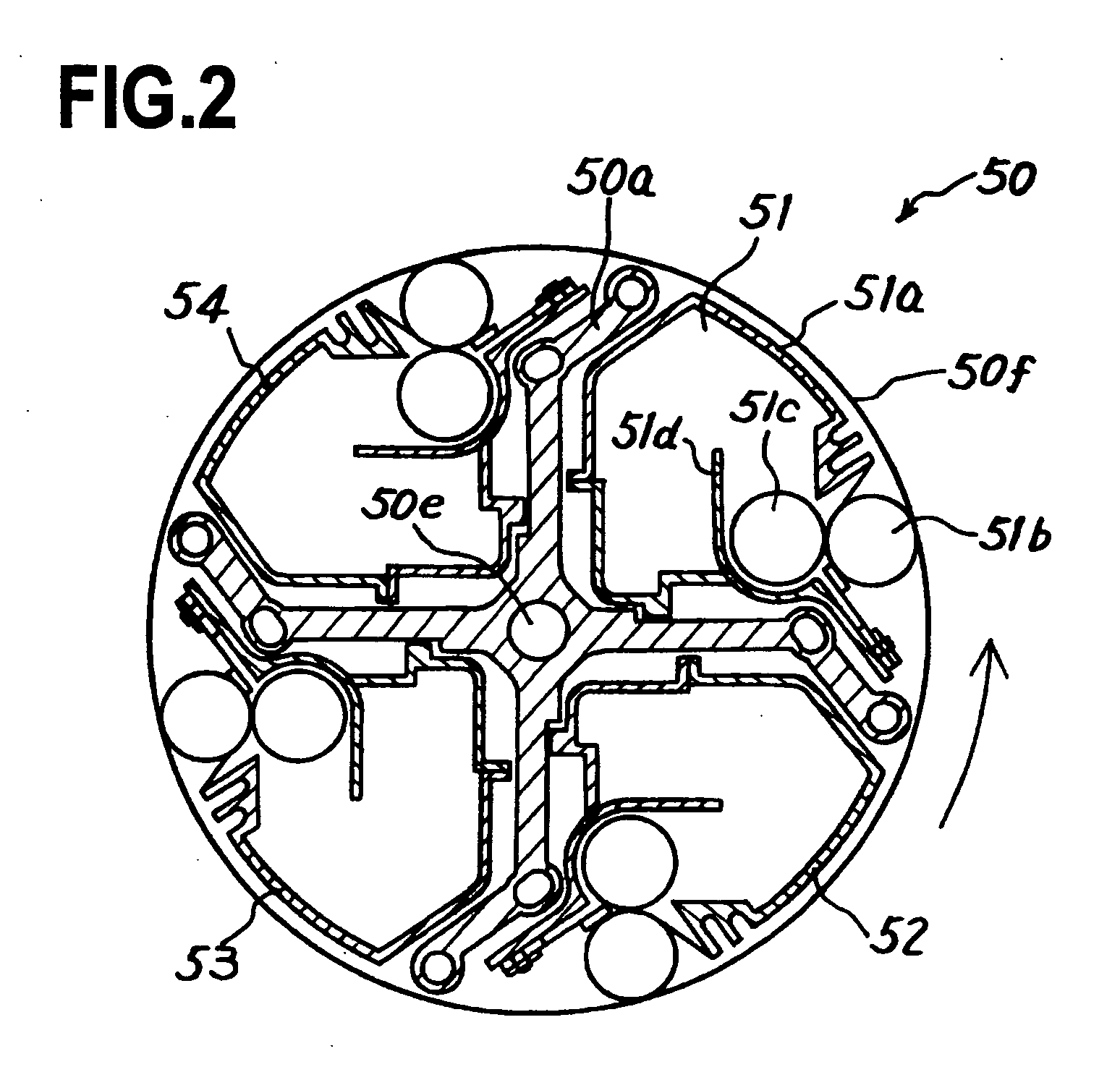
The present invention aims to provide an image forming device that reduces the calibration step by a patch pattern and simplifies the calibration process. The device includes an image carrier and a development device with multiple development units for the same color. The calibration control unit forms a predetermined patch pattern on the image carrier and develops it by attaching the developer of the development unit. The calibration control unit performs calibration by only a part of the development units or by one specific development unit. The control parameters for each development unit are determined based on the calibration result by a part of the development units and the relationship of control parameters stored in a memory. The control unit applies the control parameters to other development units. This reduces the calibration time and the amount of developer wasted.

Problems solved by technology

However this calibration step is executed in the initial step of the image forming device or when power is turned ON or when the image carrier is replaced, so if the calibration step is executed for all the development units each time, the time required for the calibration step becomes long which makes the user wait a long time, and secondly a large amount of developer is wasted in forming a patch pattern.

Method used


Image

  • Image forming device for performing calibration by patch pattern
  • Image forming device for performing calibration by patch pattern
  • Image forming device for performing calibration by patch pattern

Examples


first embodiment

[0043]FIG. 4 is a flow chart depicting the calibration control according to the In this example, in the monochrome printing mode, a specified one of the four development units is dedicated for calibration, the control parameter relational values of the four development units are detected and stored in a memory in advance, and when power is turned ON and when the photosensitive unit is replaced, calibration is performed only for the specified development unit, and the control parameters of the three development units, other than the specified development unit, are determined by the relational values between the updated control parameters of the specified development unit determined by the calibration and the control parameters stored in the memory. In other words, the control parameters of the four development units are determined and the relational values thereof are determined at the beginning, and when the power is turned ON and when the photosensitive unit is replaced thereafter...

second embodiment

[0052]FIG. 6 is a flow chart depicting the calibration control according to the Processing steps the same as FIG. 5 are denoted with the same processing numbers. In this example, at a predetermined calibration timing, such as when power is turned ON or when the exposure drum is replaced, calibration is performed not for the specified development unit but only for an arbitrary development unit. An arbitrary development unit is, for example, a development unit positioned at the development position, or a development unit which has been installed the longest time or a development unit of which the residual amount of developer is lowest at a predetermined calibration timing.

[0053] First the respective non-volatile memory is read for the installed development units as the initialization processing, and ID information, residual amount information, color information etc. are stored in the non-volatile memory 116a in the engine controller (S30). Then calibration by a patch pattern is execu...

third embodiment

[0058]FIG. 7 is a flow chart depicting the calibration control according to the In this embodiment, in the monochrome printing mode, common control parameters are used for all the development units assuming that the control parameters of all the development units are the same, and calibration is executed only for a specified development unit, and common control parameters are updated.

[0059] First as initialization processing, the information of the non-volatile memory of the installed development unit is read, and the relationship of the specified development unit and other development units and the installation positions thereof are stored in the memory (S42). Also as initialization processing, calibration by a patch pattern is executed for the specified development units, control parameters are determined based on the calibration result, and they are stored in a memory as common control parameters (S44). Since the control parameters of all the development units are used in common...


PUM


Abstract

An image forming device, has an image carrier on which a latent image is formed, and a development device to which a plurality of development units for containing developer with the same color are detachably installed, and development is performed by attaching the developer of the development unit on the latent image of the image carrier. And the image forming device further has calibration control unit for forming the latent image of a predetermined patch pattern on the image carrier, developing the image by the developer of the development unit, detecting the developed patch pattern and deciding control parameters, and the calibration control unit performs calibration by only a part of the development units or by one development unit out of the plurality of development units.

Description

BACKGROUND OF THE INVENTION [0001] 1. Field of the Invention [0002] The present invention relates to an image forming device for forming images using electronic printing technology, and more particularly to an image forming device which has a plurality of development units containing a same color developer and can simplify calibration by patch patterns. [0003] 2. Description of the Related Art [0004] An image forming device for forming images using electro-photographic technology is installed in a printer, facsimile and copier, and is comprised of an image carrier (photosensitive drum) on which an electrostatic latent image is formed according to the image data, a charge unit for charging the outer face of the image carrier, an exposure unit for exposing the charged outer face of the image carrier according to the image data and forming an electrostatic latent image, a development device for developing the electrostatic latent image of the image carrier into a toner image by supplyi...

Claims


Application Information

Patent Timeline
Patent Type & Authority Applications(United States)
IPC IPC(8): G03G15/00G03G21/00G03G15/01G03G15/06
CPCG03G2215/0161G03G15/5041G03G2215/0177
Inventor YOSHIZUKA, KENTAGUCHI, KEIICHITANAKA, HIROSHI
Owner SEIKO EPSON CORP
Learn More