Combined matching and filter circuit

a filter circuit and combined technology, applied in the field of combined matching and filter circuits, can solve the problems of difficult to obtain the required level of harmonic suppression, large circuits made using discrete components, and limited number of shunt elements in typical matching circuits, etc., to achieve the effect of increasing harmonic rejection capability and increasing harmonic rejection of circuits

Active Publication Date: 2005-12-22
MACOM TECH SOLUTIONS HLDG INC
View PDF23 Cites 131 Cited by
  • Summary
  • Abstract
  • Description
  • Claims
  • Application Information

AI Technical Summary

Benefits of technology

[0008] Briefly described, the invention provides a combined impedance matching and harmonic rejection circuit (also known as a matching filter circuit) having increased harmonic rejection capability. The increased harmonic rejection of the circuit is achieved by providing a split, or dual, resonance for one or more of the capacitive or inductive elements of the circuit.
[0010] An objective of the design is to provide matching filters with increased harmonic suppression in a more compact design that is capable of being implemented as a monolithic circuit suitable for low cost, batch manufacture.

Problems solved by technology

Circuits made using discrete components tend to be large and bulky.
Moreover, multilayer PC board ground effects tend to introduce excess inductances that make obtaining the required level of harmonic suppression difficult.
A problem of designing such combined impedance matching and filtering circuits (also known as matching filter circuits) is that there are a limited number of shunt elements in a typical matching circuit.
Such designs require a relatively large number of filter elements.
The problem, therefore, is how to design a matching filter circuit having a sufficient number of filters (also known as harmonic traps) to provide the required level of harmonic rejection, given the limited number of conductive shunt arms in a typical, low loss minimum delay matching circuit.

Method used


Image

  • Combined matching and filter circuit
  • Combined matching and filter circuit
  • Combined matching and filter circuit

Examples


Embodiment Construction

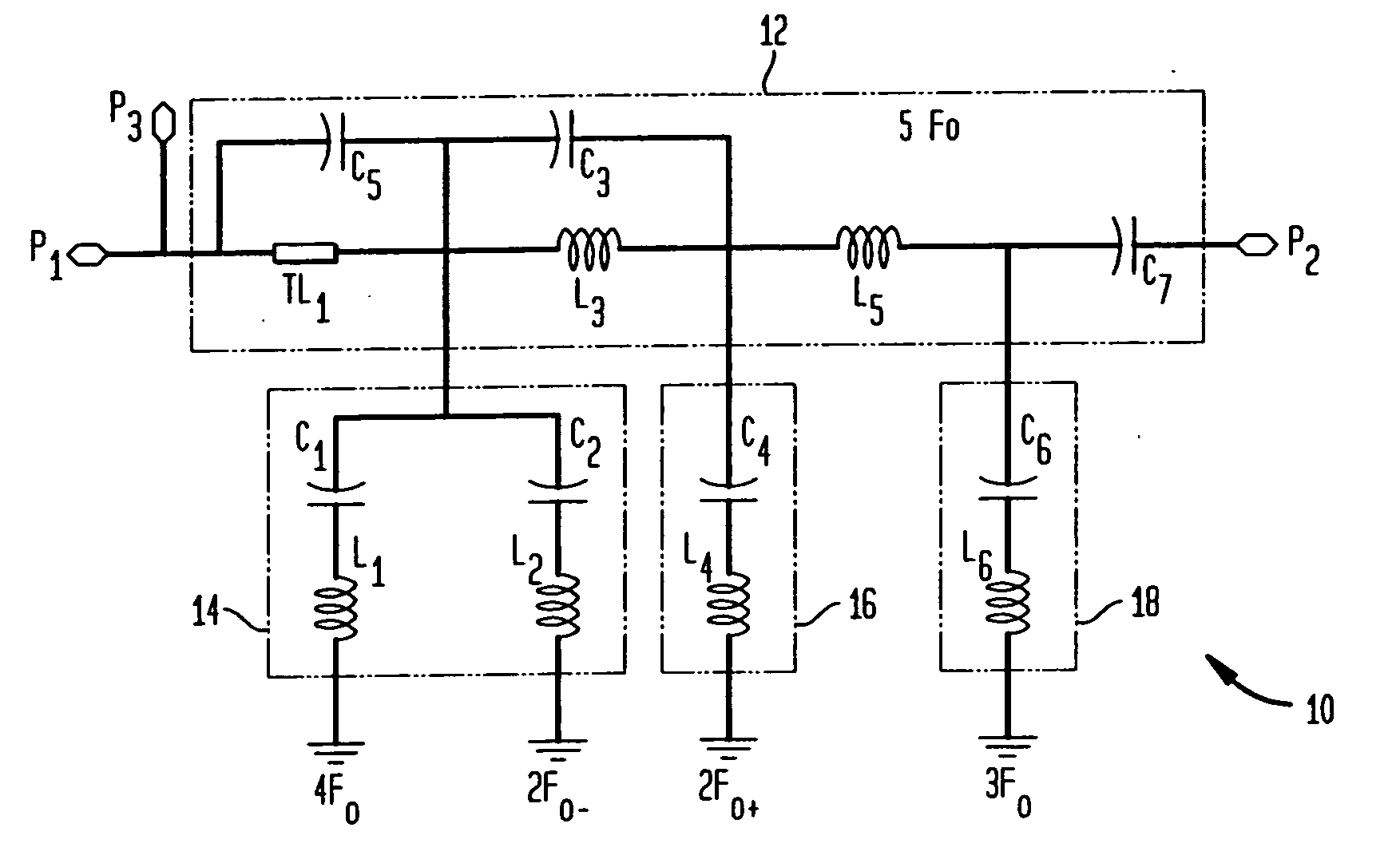
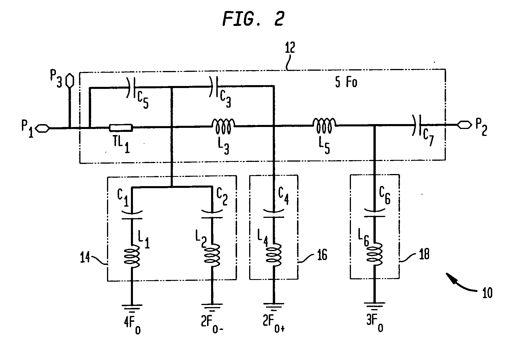
[0018] The present invention provides for combining impedance matching and harmonic filtering functions into a single match-and-filter circuit in a way that significantly improves the harmonic filtering. The invention will now be described in more detail by reference to the attached figures in which like numbers refer to like elements.

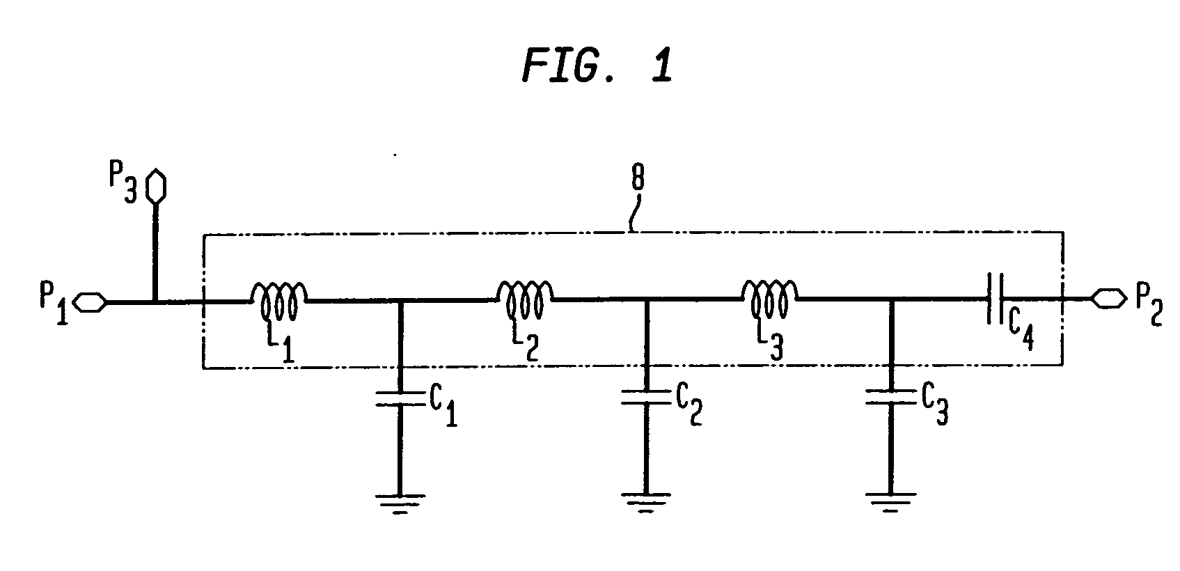
[0019]FIG. 1 is a circuit diagram of an impedance matching circuit, designed to operate at a single, fundamental frequency. The circuit has an inductive series arm 8, comprising inductors L1, L2 and L3 in series and capacitor C4. The circuit also has capacitive shunt arms, each arm including a separate capacitor C1, C2, and C3. Components L1, L2, L3, C1, C2 and C3 are chosen so that the circuit has a first effective impedance “A” at port P1 and a second, effective impedance “B” at port P2. In this way the circuit can, for instance, match an amplifier having an output impedance “A”, to a transmission line having an input impedance “B”. Capacitor C4 is ...


PUM


Abstract

A combined matching and harmonic rejection circuit with increased harmonic rejection provided by a split resonance for one or more of the capacitive or inductive elements of the circuit. At a fundamental frequency, the circuit comprises an inductive series arm with capacitive shunt arms. The capacitance of a shunt arm may be provided by two or more parallel paths, each having a capacitor and an inductor in series so that, in addition to providing the effective capacitance necessary for impedance matching at the fundamental frequency, two separate harmonics represented by the series resonances of the parallel paths are rejected. In this manner, an extra null in the circuit's stop-band may be achieved using the same number of shunt elements necessary to achieve impedance matching at the fundamental frequency.

Description

FIELD OF THE INVENTION [0001] The present invention relates to impedance matching and harmonic filtering for power amplifiers, and in particular to impedance matching and harmonic filtering for cellular phone transmission amplifiers. BACKGROUND OF THE INVENTION [0002] Cellular phones typically transmit at radio frequencies (RF) in the 1 to 5 GHz range. At these frequencies, transmission lines have an impedance of approximately 50 Ohms, while typical cellular phone transmission power amplifiers have output impedances in the range of 1 to 5 Ohms. Cellular phones therefore require an impedance matching circuit between their power amplifiers and transmission lines. [0003] In addition, regulatory bodies such as the Federal Communications Commission (FCC) have strict regulations regarding harmonic suppression in cellular phones. This suppression, if properly implemented, prevents cellular phone use from interfering with communications equipment operating at the higher frequencies harmonic...

Claims


Application Information

Patent Timeline
Patent Type & Authority Applications(United States)
IPC IPC(8): H03H2/00H03H7/01H03H7/09H03H7/38
CPCH03H7/0115H03H7/0123H03H7/1758H03H7/1766H03H2001/0078H03H7/1791H03H7/38H03H2001/0064H03H7/1783
Inventor ONNO, PETERRAJANISHJAIN, NITINWEIGAND, CHRISTOPHER D.
Owner MACOM TECH SOLUTIONS HLDG INC
Why Eureka
Try Eureka