GaAs technology K wave band frequency converter structure chip

A structure chip, K-band technology, applied in the field of GaAs process K-band inverter structure chip, can solve the problems of low harmonic suppression, low output frequency, and few functions, achieve good power flatness, and overcome technical difficulties , good effect of each harmonic suppression degree

Inactive Publication Date: 2021-06-08
HEFEI IC VALLEY MICROELECTRONICS CO LTD
View PDF4 Cites 0 Cited by
  • Summary
  • Abstract
  • Description
  • Claims
  • Application Information

AI Technical Summary

Problems solved by technology

The defects in the existing technology are: fewer functions, K-band local oscillator amplification structure that is difficult to realize in traditional circuits, low output frequency, low harmonic suppression and large size, etc.

Method used


Image

  • GaAs technology K wave band frequency converter structure chip
  • GaAs technology K wave band frequency converter structure chip
  • GaAs technology K wave band frequency converter structure chip

Examples


Embodiment

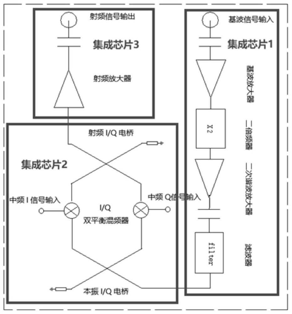
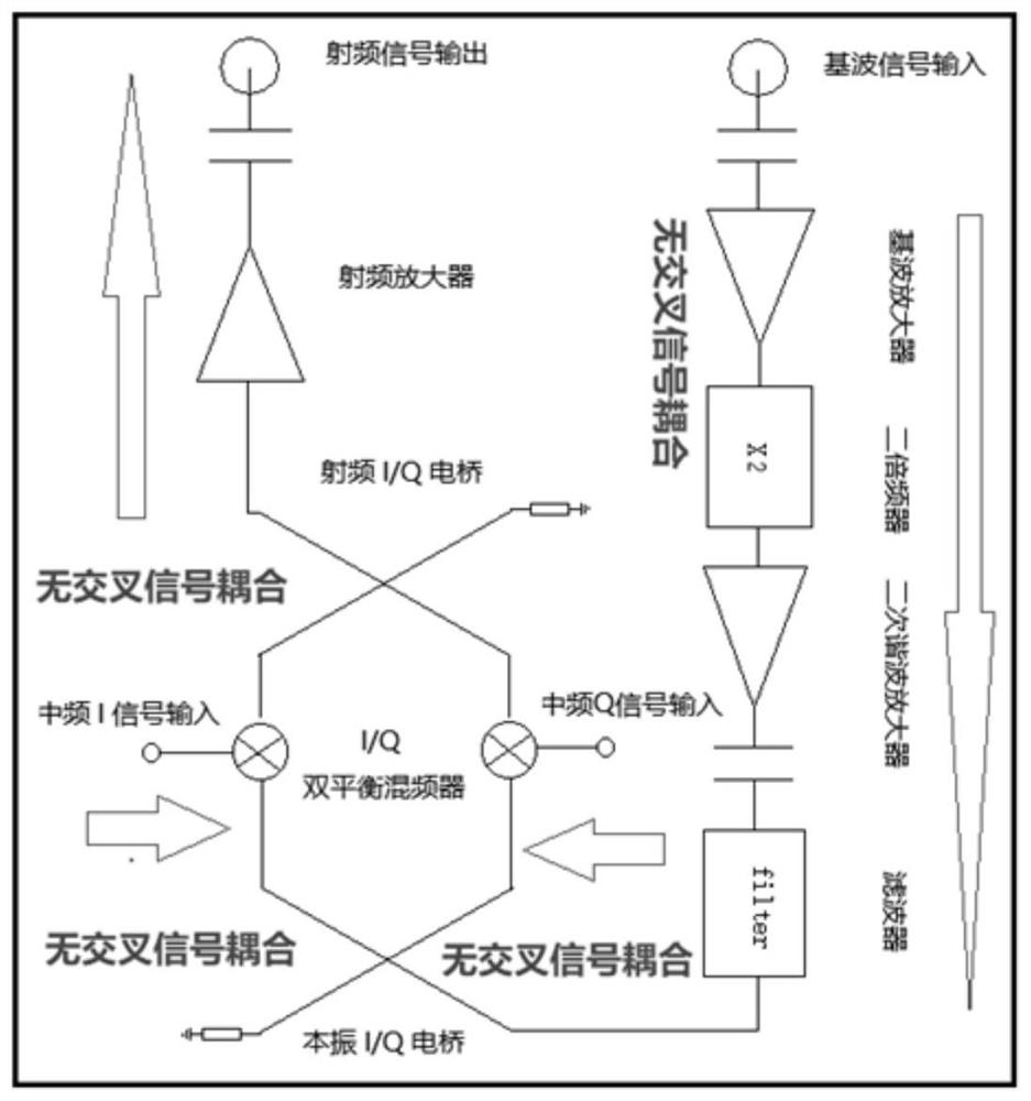
[0021] see Figure 1 to Figure 4 , the present invention provides a technical solution:

[0022] A new type of GaAs process K-band inverter structure chip, which is characterized in that the chip integrates a local oscillator frequency doubling amplification filter circuit, a local oscillator RF Lange bridge, a double-balanced mixer and a radio frequency amplifier in the GaAs single-chip K-band.

[0023] The circuit structure is clear and clear. For the first time in China, the K-band single chip integrates multiple functions such as amplification, frequency doubling, and filtering. It realizes the double frequency multiplier in the K-band, and realizes the K-band local oscillator amplification that is difficult to achieve with traditional circuits. Structure, integrated double-balanced frequency mixing, RF amplification function, with high output frequency, high harmonic suppression and small size and so on.

[0024] The present invention integrates discrete single-function ...


PUM


Abstract

The invention provides a GaAs process K wave band frequency converter structure chip, the working frequency is 17.7 GHz-23.4 GH, the fundamental wave signal input frequency is 8.85 GHz-11.7 GHz, an input signal is amplified through a fundamental wave amplifier, the amplified signal drives a frequency doubler to work, the signal is subjected to secondary frequency doubling, and clutters are further filtered out through a filter. The frequency multiplication function from the X wave band to the K wave band is achieved, the output power of 16 dBm is achieved, the power flatness is good, and the harmonic suppression degree of each order is good and reaches 55 dBc. An amplified local oscillator signal is divided into two paths of signals with the phase difference of 90 degrees through a local oscillator I / Q bridge, the two paths of signals enter a frequency mixer and a double-balanced frequency mixer respectively to be mixed with an input intermediate frequency I signal and an input intermediate frequency Q signal respectively, the mixed signals enter a radio frequency I / Q bridge to be synthesized, mirror image signals are effectively suppressed, and the suppression degree reaches 50 dBc. The radio-frequency signal finally enters the low-noise radio-frequency amplifier, the output power is larger than 17 dBm, the noise is smaller than 10 dB, and 0.05 W radio-frequency power output is achieved.

Description

technical field [0001] The invention relates to the technical field of a multifunctional K-band up-converter, in particular to a GaAs process K-band frequency converter structure chip. Background technique [0002] All the K-band up-converter chips in the prior art are single-function circuits. Single-function circuits such as figure 1 As shown, it is one of the integrated chips 1-3, and the current area of ​​a single integrated chip 1 is roughly 2×2mm 2 , the area of ​​the integrated chip 2 is roughly 1.6×2mm 2 , the single area of ​​the integrated chip 3 is roughly 1.6×1.6mm 2 . The defects in the prior art include: fewer functions, a K-band local oscillator amplification structure that is difficult to realize in traditional circuits, low output frequency, low harmonic suppression, and large size. Contents of the invention [0003] The purpose of the present invention is to provide a GaAs process K-band frequency converter structure chip to solve the problems raised...

Claims


Application Information

Patent Timeline
Patent Type & Authority Applications(China)
IPC IPC(8): H03D7/16
CPCH03D7/16
Inventor 黄军恒
Owner HEFEI IC VALLEY MICROELECTRONICS CO LTD
Why Eureka
Try Eureka