
Eureka
For R&D, Eureka makes reading and utilizing patents & technical documents easy.
Eureka AIR
Designed for self-driven R&D workflows. Generate viable solutions, solve complex R&D challenges, empower your innovation with AI.

Eureka Materials
Designed for material experts only. Revolutionize your material R&D, from search, analyze, to developing new materials.

TechResearch
Generate reliable direction feasibility study reports for your R&D in just a few steps.

TechSeek
Discover and master advanced knowledge NOW. Basics, ideas, possibilities, all at once.

TechMind
As an expert in R&D Theories, TechMind can generates customized viable solutions instantly.

TechRisk
Analyze your overall solution with one click, know your potential R&D risks in advance.

TechMonitor
Get weekly tech updates, stay abreast of the latest tech innovations and key insights.
Semiconductor device
- Summary
- Abstract
- Description
- Claims
- Application Information
AI Technical Summary
Benefits of technology
Problems solved by technology
Method used
Image

Examples
embodiment 1
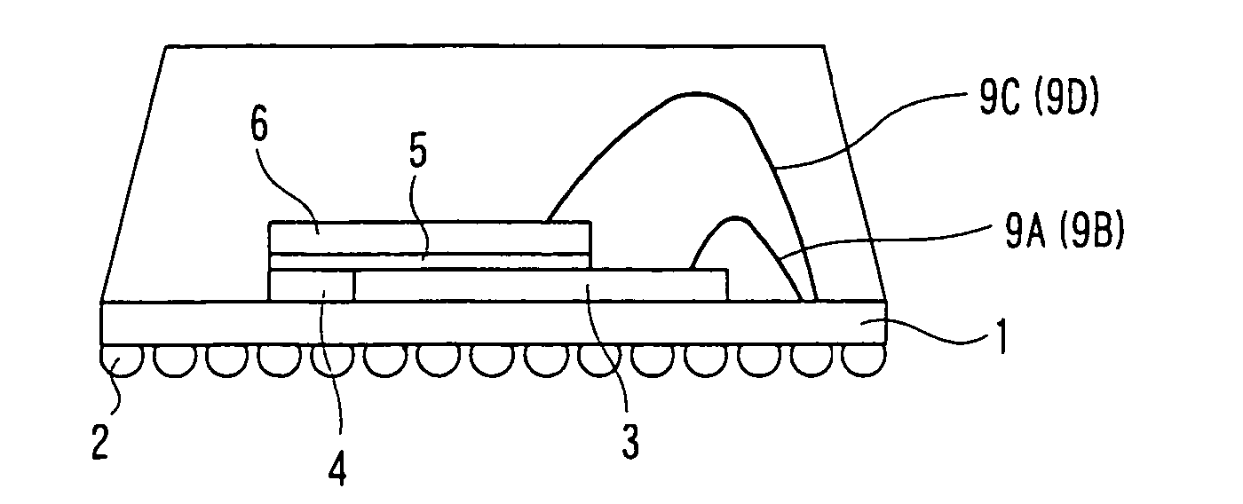
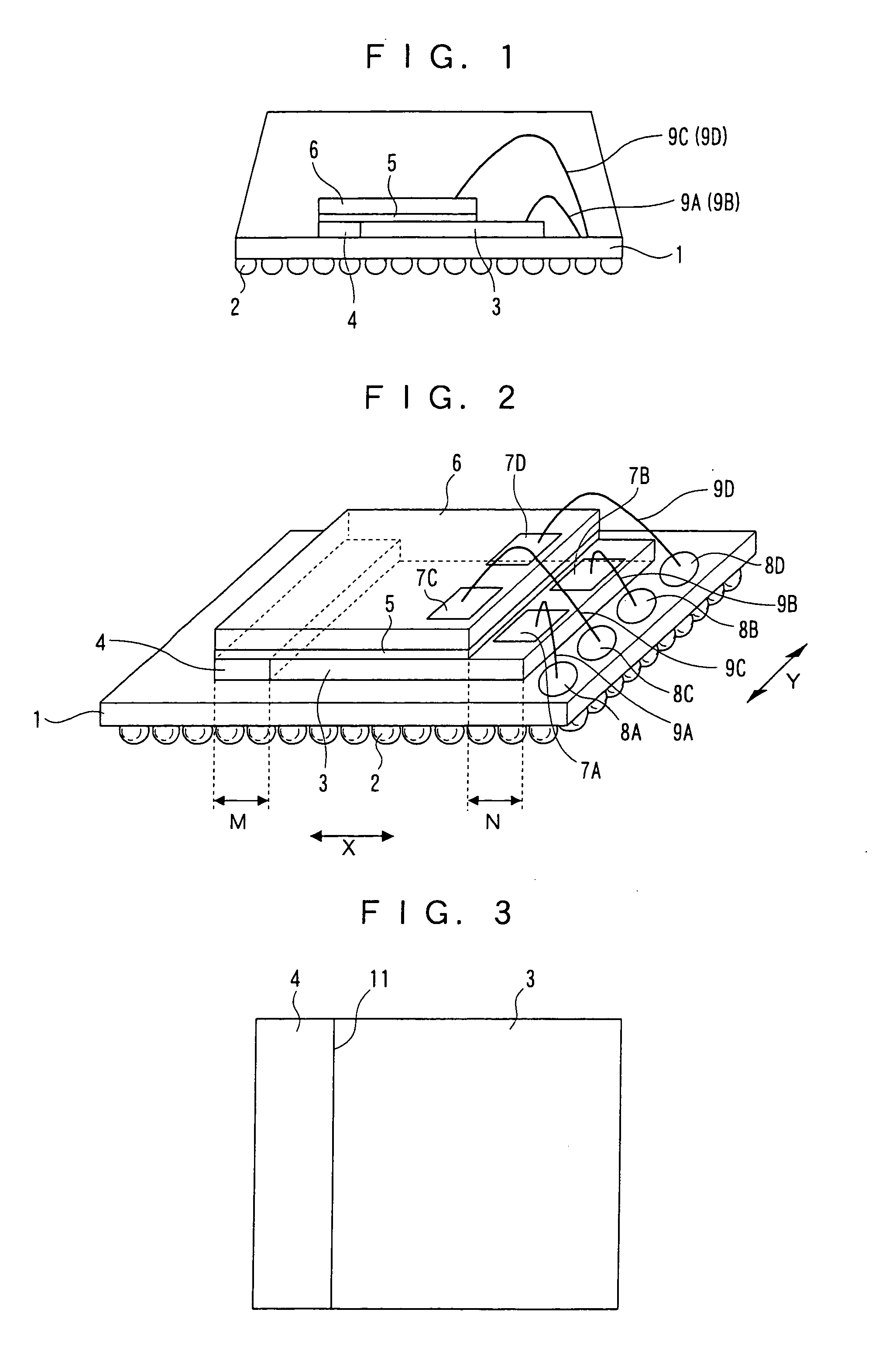
[0018] As shown in FIGS. 1 and 2, a semiconductor device according to Embodiment 1 of the present invention comprises a substrate 1, external electrodes 2, a first semiconductor chip 3, a spacer 4, an insulating film 5, a second semiconductor chip 6, a first pad 7A, a second pad 7B, a third pad 7C, a fourth pad 7D, a first electrode 8A, a second electrode 8B, a third electrode 8C, a fourth electrode 8D, a first wire 9A, a second wire 9B, a third wire 9C, and a fourth wire 9D.
[0019] The substrate 1 s composed of an inorganic composite (e.g., a ceramic substrate and a glass substrate) and has a plurality of wiring patterns formed on one surface (the top surface in the vertical direction). The substrate 1 is formed with a single layer.
[0020] The external electrodes 2 are disposed on the other surface (the undersurface in the vertical direction) of the substrate 1 and are connected to other components.
[0021] The first semiconductor chip 3 is mounted on one surface (top surface) of th...
embodiment 2
[0050] Referring to FIG. 7, the following will describe a semiconductor device using a first semiconductor chip and a spacer according to Embodiment 2 of the present invention.
[0051] As shown in FIG. 7, the semiconductor device of Embodiment 2 comprises a substrate 31, external electrodes 32, a first semiconductor chip 33, a first spacer 34A, a second spacer 34B, an insulating film 35, a second semiconductor chip 36, a first pad 37A, a second pad 37B, a third pad 37C, a fourth pad 37D, a fifth pad 37E, a sixth pad 37F, a seventh pad 37G, an eighth pad 37H, a first electrode 38A, a second electrode 38B, a third electrode 38C, a fourth electrode 38D, a first wire 39A, a second wire 39B, a third wire 39C, and a fourth wire 39D.
[0052] The substrate 31 is composed of an inorganic composite (e.g., a ceramic substrate and a glass substrate) and has a plurality of wiring patterns formed on one surface (the top surface in the vertical direction). The substrate 31 is formed with a single la...
PUM
 Abstract
Description
Claims
Application Information
 - R&D Engineer
- R&D Manager
- IP Professional
- Industry Leading Data Capabilities
- Powerful AI technology
- Patent DNA Extraction
Browse by: Latest US Patents, China's latest patents, Technical Efficacy Thesaurus, Application Domain, Technology Topic, Popular Technical Reports.
© 2024 PatSnap. All rights reserved.Legal|Privacy policy|Modern Slavery Act Transparency Statement|Sitemap|About US| Contact US: help@patsnap.com