Device, method, and program for computer aided design of flexible substrates

a flexible printed circuit board and computer-aided design technology, applied in the direction of cad circuit design, coupling device connection, instruments, etc., can solve problems such as error notification

Inactive Publication Date: 2005-12-29
PANASONIC CORP
View PDF16 Cites 20 Cited by
  • Summary
  • Abstract
  • Description
  • Claims
  • Application Information

AI Technical Summary

Benefits of technology

[0015] This device estimates the position of a part when the flexible printed circuit board is bent at the bend position with the flexible printed circuit board in an unbent state. That is, the position of the part when the flexible printed circuit board is bent is calculated as the prohibited space. The prohibited space generated by a first part is compared to the space occupied by a second part on the printed circuit board. By means of this comparison, when the first part and second part contact one another, or a predetermined clearance is not maintained between the first part and second part, and an error notification is output as a design standard violation. In this way, the interference of parts, such as contact between parts when the flexible printed circuit board is bent, can be easily considered in the design even when the flexible printed circuit board is in an unbent state.
[0017] The prohibited space has at least the same size as the space occupied by the first part, that is, the same height and planar area. In this way, it is possible to estimate the influence exerted on the surface opposite the first part when the flexible printed circuit board is bent.
[0021] By visually outputting the prohibited space, it is possible to aid smooth printed circuit board design by preventing, beforehand, the placement of a new part at a position which will generate a design standard violation. An example of this visual output is a projection of the prohibited space displayed on the printed circuit board.
[0025] When a new part is installed on the printed circuit board, an error notification is output if the new part is within a previously established prohibited space. In this way placing a new part at a position which will generate a design standard violation can be easily avoided. When a new part is placed outside a pre-existing prohibited space, it is desirable that a new prohibited space is generated at a position of axial symmetry relative to the part centered at the bend position.

Problems solved by technology

By means of this comparison, when the first part and second part contact one another, or a predetermined clearance is not maintained between the first part and second part, and an error notification is output as a design standard violation.

Method used


Image

  • Device, method, and program for computer aided design of flexible substrates
  • Device, method, and program for computer aided design of flexible substrates
  • Device, method, and program for computer aided design of flexible substrates

Examples


first embodiment

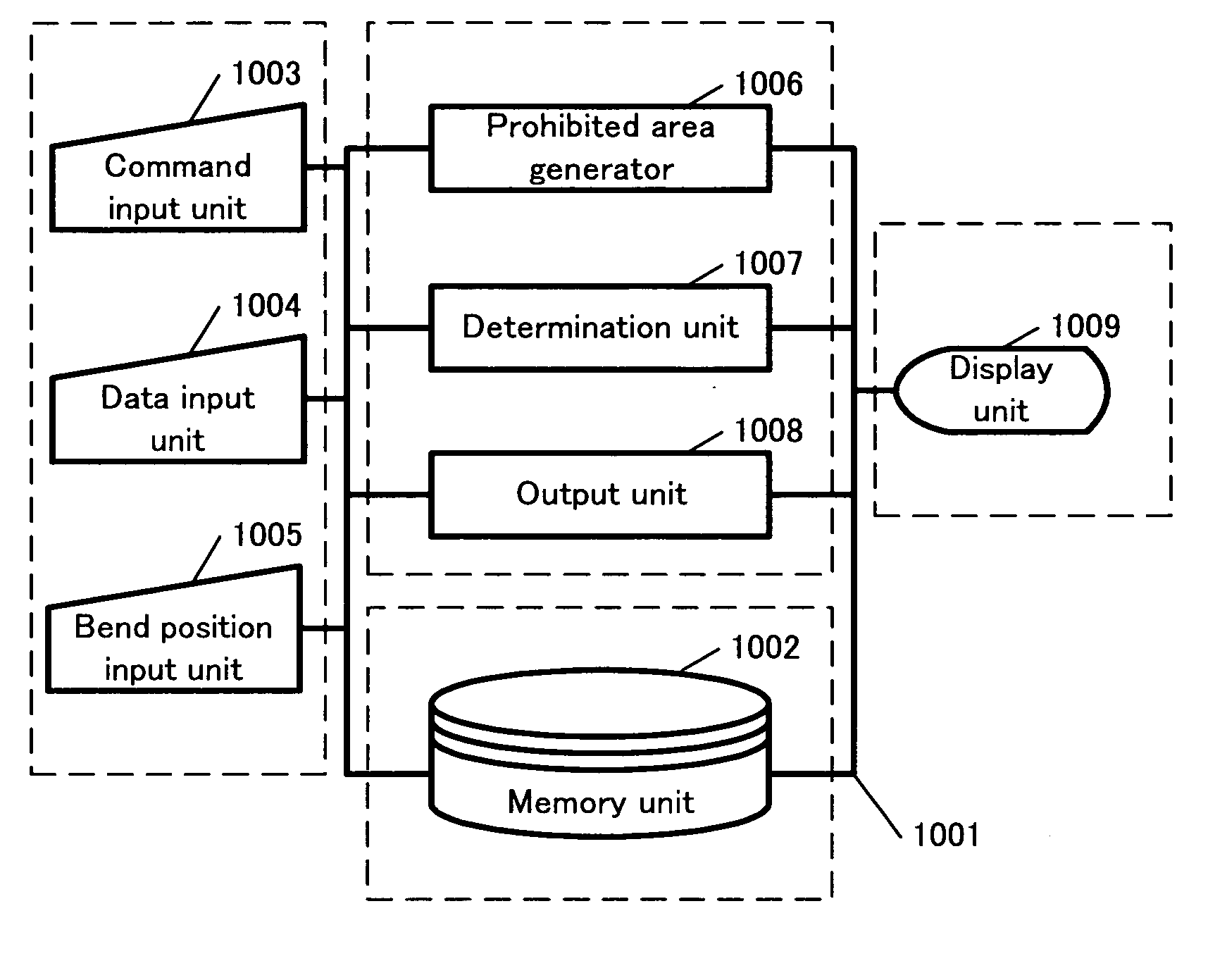
[0069] 1. Structure 1-1. General Structure FIG. 1 shows a structural diagram of the functions of a device for computer aided design of the present embodiment. A computer aided design device 1001 is equivalent to a CAD system used for PCB (printed circuit board) layout design. The layout designer creates layout data using this device.

[0070] The computer aided design device 1001 includes a memory unit 1002, command input unit 1003, data input unit 1004, bend position input unit 1005, prohibited area generator 1006, determination unit 1007, and output unit 1008. The computer aided design device 1001 is connected to a display unit 1009 which provides a display. The computer aided design device 1001 is achieved by a computer provided with hardware such as a CPU, ROM, RAM, and a memory device. The functions of each part are specifically described below.

[0071] 1-2 Memory Unit

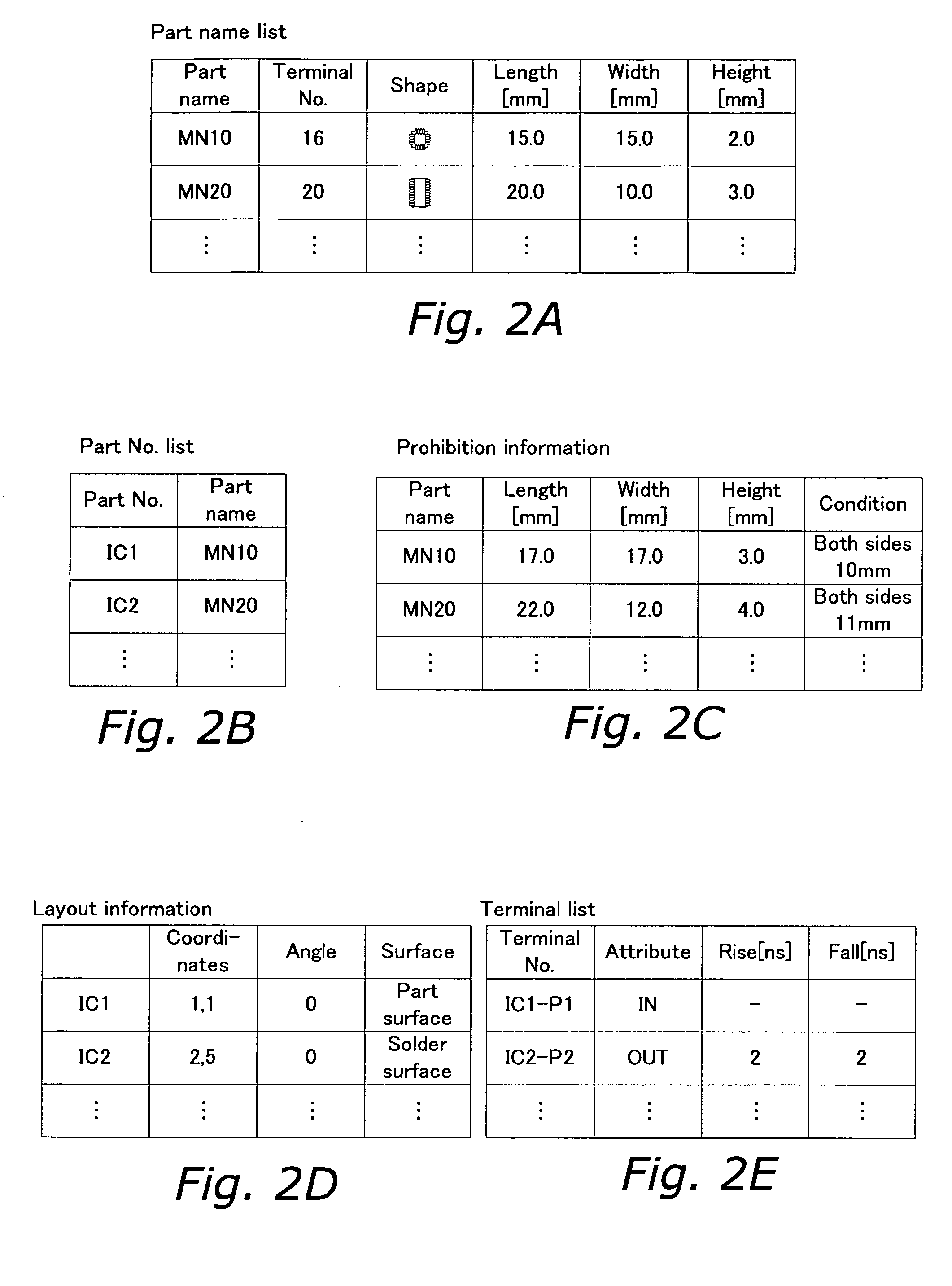
[0072] The memory unit 1002 stores design data including part information (equivalent to part data), prohibition ...


PUM


Abstract

A device, method, and program too facilitate the design of flexible printed circuit boards is disclosed which generates, as a prohibited space, a position assumed to be occupied by a part on an opposing printed circuit board when the printed circuit board is bent from a bend position. Design preparation of a bendable flexible printed circuit board can be efficiently checked by checking for the presence / absence of interference between parts and prohibited spaces.

Description

BACKGROUND OF THE INVENTION [0001] 1. Field of the Invention [0002] The present invention relates a device for computer aided design of flexible printed circuit boards. More specifically, the present invention relates to computer aided design of bendable flexible printed circuit boards. [0003] 2. Background Information [0004] In conventional computer aided design of flexible substrates, the flexible substrate is designed using flat printed circuit board (PCB) computer aided design (CAD). [0005] Japanese Patent Application Publication No. 2002-117082 discloses a device for simulating the mounting of a flexible printed substrate. This device checks whether or not the deformation limit of a part is exceeded when the substrate is deformed, and outputs a message when the deformation limit is exceeded. [0006]FIG. 12 is a flow chart of the process of simulating the mounting of a flexible printed substrate disclosed in Japanese Patent Application Publication No. 2002-117082. The mounting si...

Claims


Application Information

Patent Timeline
Patent Type & Authority Applications(United States)
IPC IPC(8): G06F17/50H01R25/00H05K1/00H05K3/00
CPCG06F17/5068H05K3/0005H05K1/0393G06F2217/40G06F2113/18G06F30/39
Inventor NAKAYAMA, TAKESHITANIMOTO, SHIN-ICHISAITO, YOSHIYUKI
Owner PANASONIC CORP
Why Eureka
Try Eureka