

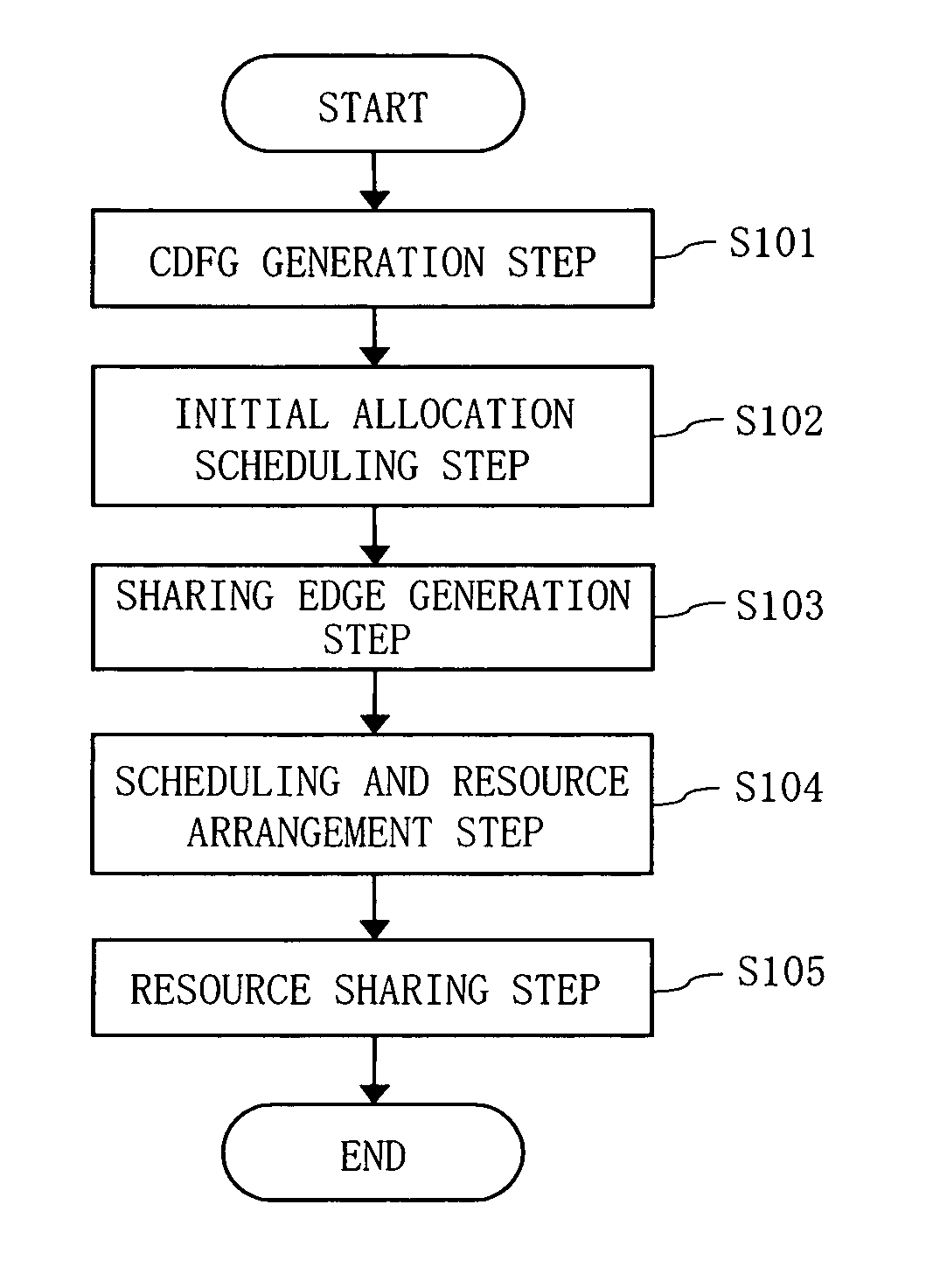
High level synthesis method for semiconductor integrated circuit
a technology of integrated circuits and synthesis methods, applied in the direction of cad circuit design, program control, instruments, etc., can solve the problems of difficult to complete layout design and physical design, difficulty in ensuring the completion of circuit design on the one hand, and inapplicability of solutions, so as to achieve efficient sharing of allocated resources
- Summary
- Abstract
- Description
- Claims
- Application Information
AI Technical Summary
Benefits of technology
Problems solved by technology
Method used
Image

Examples
first embodiment
Fourth Variant of First Embodiment
[0179]FIG. 35 is a flowchart showing a layout-based high level synthesis method according to a fourth variant of the first embodiment of the present invention. In the flowchart shown in FIG. 35, an attraction force sharing edge weight adjustment step (step S131) is added between the sharing edge generation step (step S103) and the scheduling and resource arrangement step (step S104) in the flowchart shown in FIG. 1. Identical steps to those of FIG. 1 bear the same step numbers and will not be described here.
[0180] With the high level synthesis method according to this variation, the attraction force sharing edge weight adjustment step (step S131) is performed after the sharing edge generation step (step S103). In the attraction force sharing edge weight adjustment step, the weight given to the attraction force sharing edge generated in the sharing edge generation step is changed in accordance with certain criteria.
[0181] In the sharing edge genera...
second embodiment
[0208]FIG. 41 is a flowchart showing a layout-based high level synthesis method according to a second embodiment of the present invention. According to the high level synthesis method shown in FIG. 41, a CDFG generation step, an initial allocation scheduling step, an attraction force sharing edge generation step, an attraction force sharing edge thinning step, a resource arrangement step, and an incremental improving resource sharing step are performed for operation description data describing the operation specifications of a design target circuit.
[0209] In FIG. 41, the CDFG generation step (step S201) and the initial allocation scheduling step (step S202) are the same as those included in the high level synthesis method (FIG. 1) according to the first embodiment, and will not be described here.
[0210] In the attraction force sharing edge generation step (step S203), a new sharing edge is added between sharable allocated resources included in allocated resource connection graph wh...
PUM
 Abstract
Description
Claims
Application Information