System and method for lithography process monitoring and control

a technology of process monitoring and control, applied in the field of lithographic systems and techniques, can solve the problems of reducing the use of photomasks, affecting the quality of lithography, and affecting the quality of lithography, and achieve the effect of high precision movemen

Inactive Publication Date: 2006-01-05
ASML NETHERLANDS BV
View PDF9 Cites 111 Cited by
  • Summary
  • Abstract
  • Description
  • Claims
  • Application Information

AI Technical Summary

Benefits of technology

[0022] In another principal aspect, the present invention is an image sensor unit, for use with a highly precise moveable platform, which includes a wafer-shaped substrate and a sensor array, integrated into the substrate. The sensor array includes a plurality of sensor cells (for example, charge coupled devices, CMOS devices or photodiodes) wherein each sensor cell includes an active area to sense light of a predetermined wavelength that is incident thereon. The sensor array also includes a film, disposed over the plurality of active areas of the sensor cells and comprised of a material that impedes passage of light of the predetermined wavelength. The film includes a plurality of apertures that are arranged such that an aperture of the plurality of apertures overlies an active area of a corresponding sensor cell to expose a portion of the active area. In this way, light of the predetermined wavelength is capable of being sensed by the portion of the active area that is exposed by the corresponding aperture.

Problems solved by technology

While such inspection equipment may provide an accurate representation of the photomask, it tends to be quite expensive and hence its use tends to be minimized.
Moreover, such inspection equipment often employs optical imaging systems (or sub-systems) that are fundamentally different from that used by the stepper in “printing” the image on the wafer during mass production.
Indeed, a photomask may exhibit defects in the production stepper environment that may not be detectable in the standalone inspection tool because, for example, detection of certain contaminants depends on wavelength.
That is, certain contaminants may present serious issues at the wavelength used during production but may be undetectable at the wavelength used during inspection.
Due primarily to complexity of the inspection techniques, the inspection procedure of the stepper tends to require or consume an extended period of time, often days to complete, and thus represents an expensive procedure for the integrated circuit manufacturer to carry out.
Here again, due to the extended test time, inspection of the stepper is not performed very often, and, as a result, there are few samples and / or data to form a reliable measure of the stepper.
Because the final printed circuit pattern on the wafer or die is formed after the resist development and may be after substrate treatment (for example, material etching or deposition), it may be difficult to attribute, discriminate or isolate errors in the final printed circuit pattern to problems associated with the photomask, the stepper, or the resist deposition and / or the developing processes.
Moreover, as with inspection of the optics of the stepper, inspecting the final printed circuit pattern on the wafer or die using an SEM tends to offer a limited number of samples upon which to detect, determine, and resolve any processing issues.
This process may be labor intensive and presents an extensive inspection and analysis time.

Method used


Image

  • System and method for lithography process monitoring and control
  • System and method for lithography process monitoring and control
  • System and method for lithography process monitoring and control

Examples


Embodiment Construction

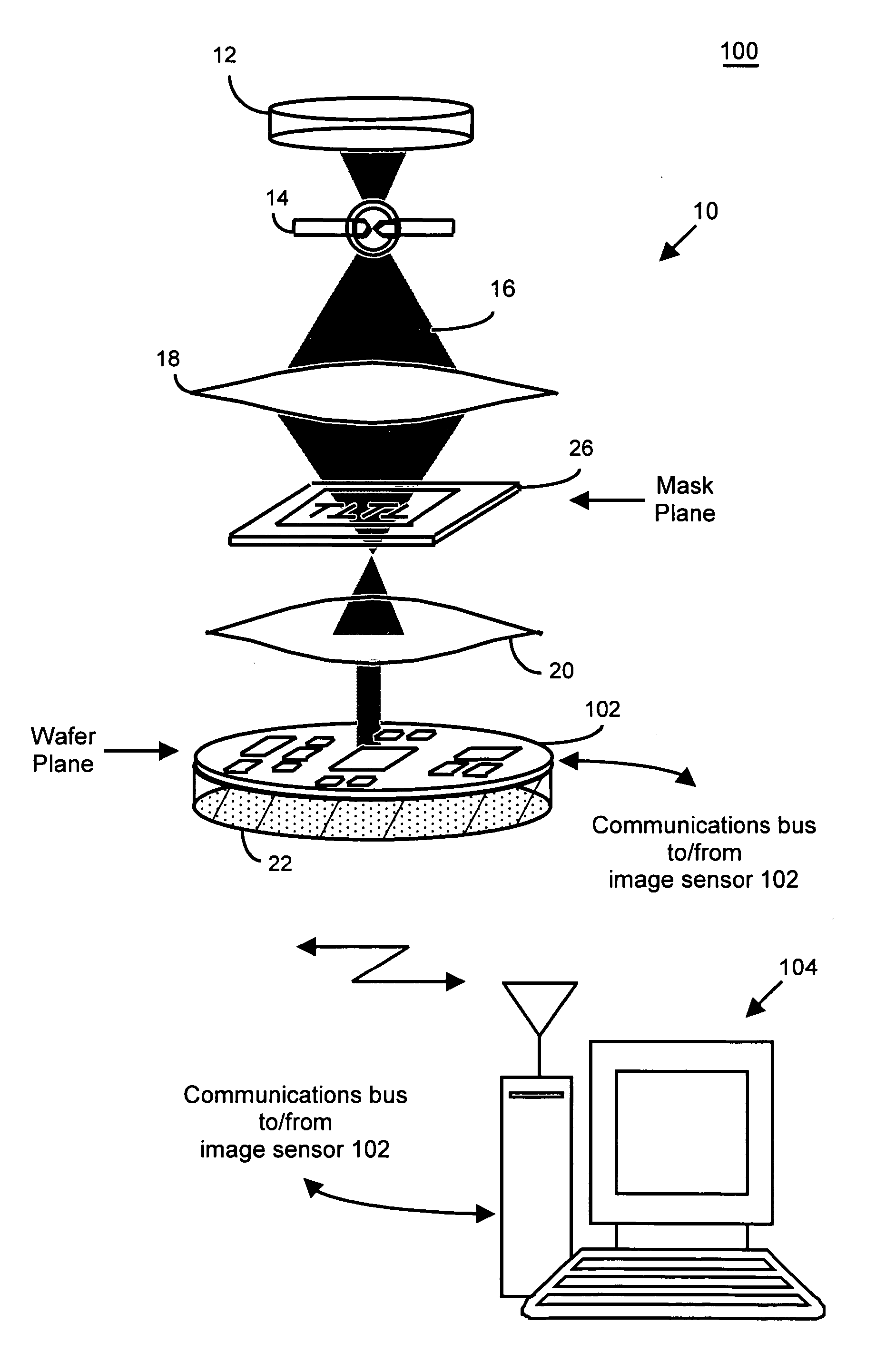
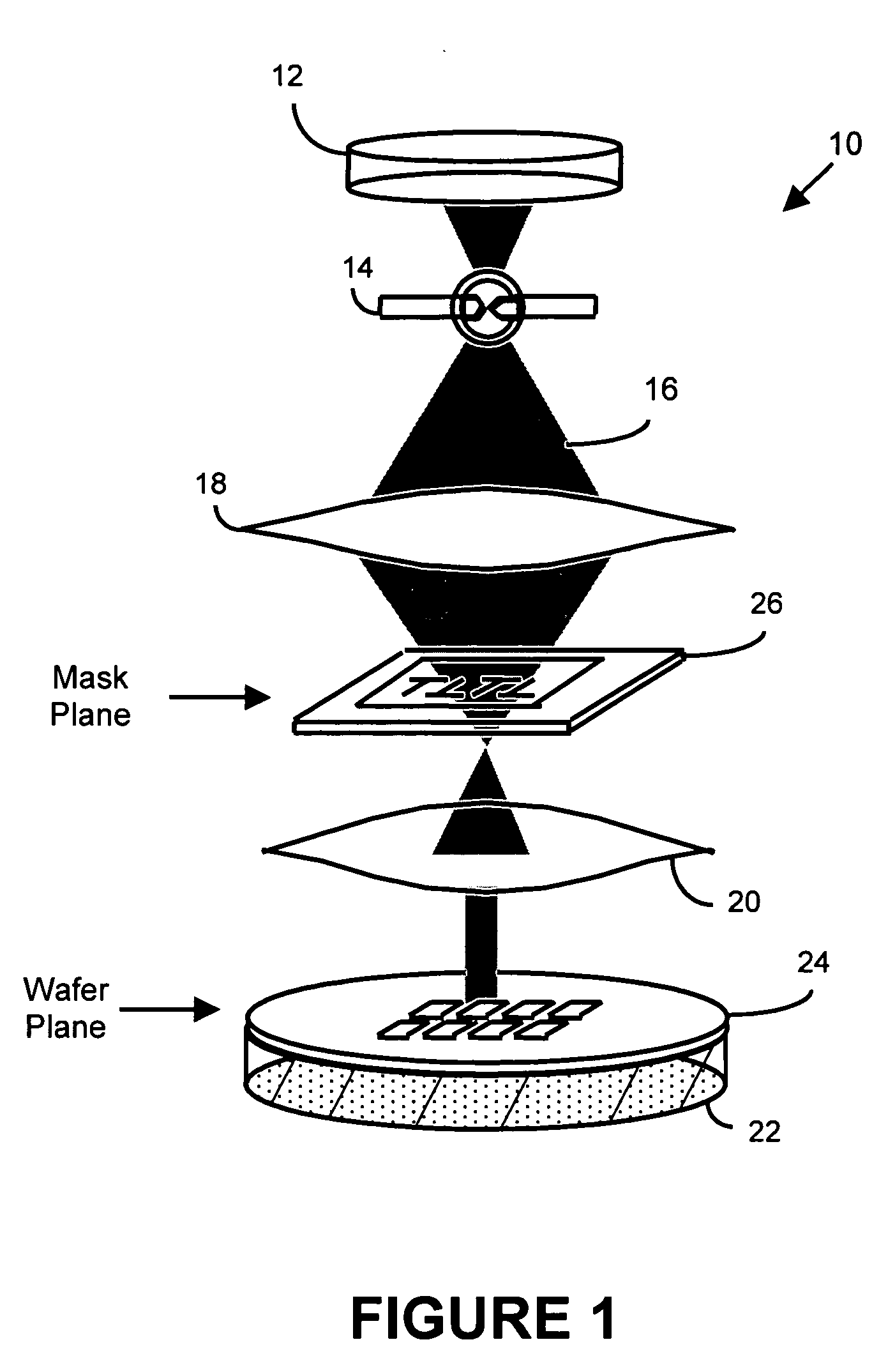
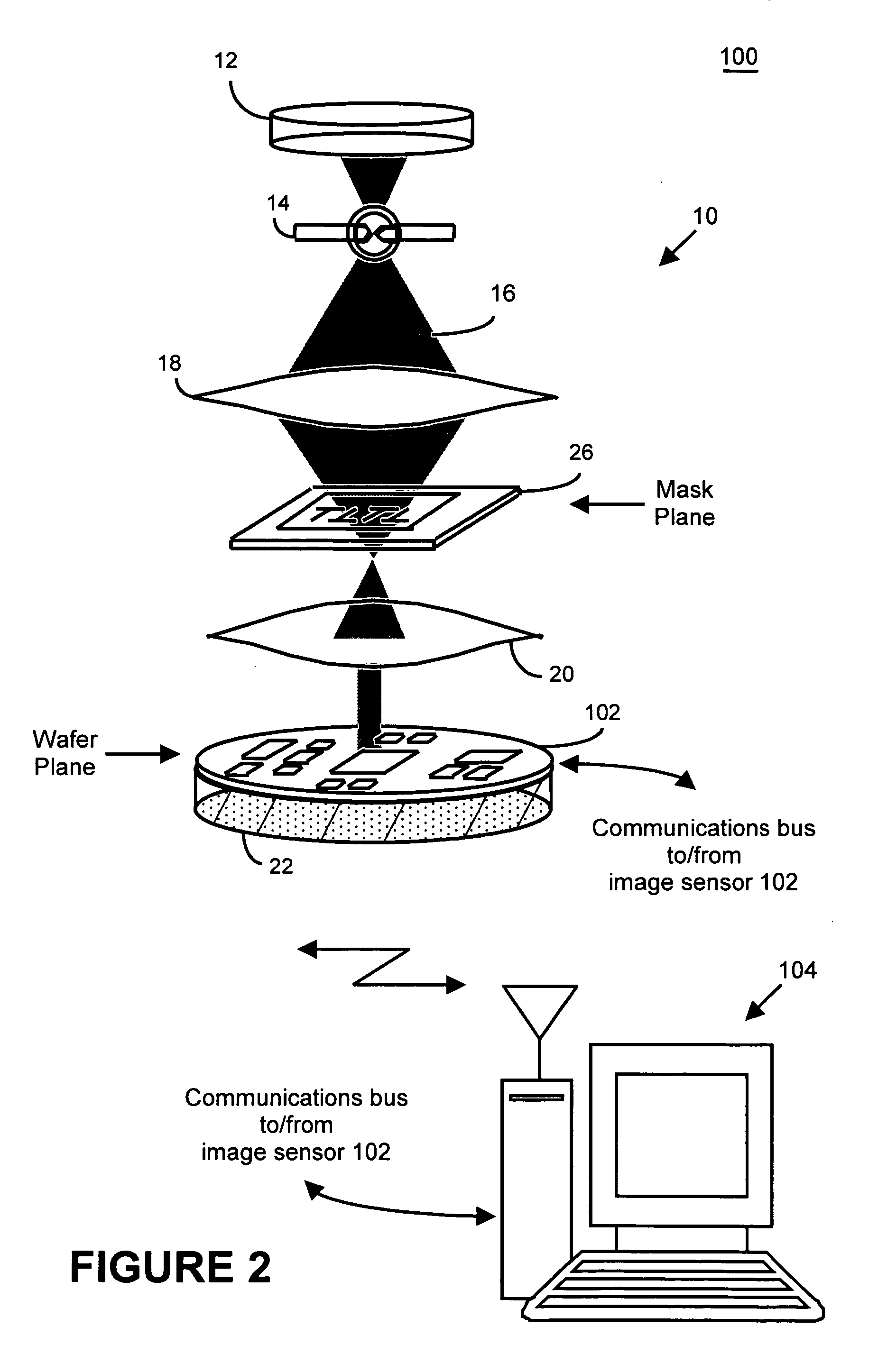
[0054] There are many inventions described herein. In one aspect, the present invention is directed to a technique of, and system for measuring, inspecting, characterizing and / or evaluating optical lithographic equipment, methods, and / or materials used therewith, for example, photomasks. In this regard, the present invention is a system, sensor and technique to sample, measure, collect and / or detect an aerial image produced or generated by the interaction between the photomask and lithographic equipment. An image sensor unit may be employed to sample, measure, collect and / or detect the aerial image of a product-type photomask (i.e., a photomask that is used in the production of integrated circuits on product wafers) in situ—that is, the aerial image at the wafer plane produced by the interaction between the photomask and the lithographic equipment that are used (or to be used) during manufacture of integrated circuits. In this way, the aerial image used, generated or produced to mea...


PUM


Abstract

In one aspect, the present invention is a technique of, and a system and sensor for measuring, inspecting, characterizing and / or evaluating optical lithographic equipment, methods, and / or materials used therewith, for example, photomasks. In one embodiment, the system, sensor and technique measures, collects and / or detects an aerial image produced or generated by the interaction between the photomask and lithographic equipment. An image sensor unit may measure, collect, sense and / or detect the aerial image in situ—that is, the aerial image at the wafer plane produced, in part, by a product-type photomask (i.e., a wafer having integrated circuits formed during the integrated circuit fabrication process) and / or by associated lithographic equipment used, or to be used, to manufacture of integrated circuits. In this way, the aerial image used, generated or produced to measure, inspect, characterize and / or evaluate the photomask is the same aerial image used, generated or produced during wafer exposure in integrated circuit manufacturing. In another embodiment, the system, sensor and technique characterizes and / or evaluates the performance of the optical lithographic equipment, for example, the optical sub-system of such equipment. In this regard, in one embodiment, an image sensor unit measures, collects, senses and / or detects the aerial image produced or generated by the interaction between lithographic equipment and a photomask having a known, predetermined or fixed pattern (i.e., test mask). In this way, the system, sensor and technique collects, senses and / or detects the aerial image produced or generated by the test mask—lithographic equipment in order to inspect, evaluate and / or characterize the performance of the lithographic equipment.

Description

CROSS-REFERENCE TO RELATED APPLICATIONS [0001] This application claims priority to: (1) U.S. Provisional Application Ser. No. 60 / 386,408, entitled “Complete Optical Lithography Inspection and Process Control”, filed Jun. 7, 2002; and (2) U.S. Provisional Application Ser. No. 60 / 432,725, entitled “Method and Apparatus for Aerial Imaging”, filed Dec. 12, 2002. The contents of these provisional applications are incorporated by reference herein in their entirety.BACKGROUND OF THE INVENTION [0002] This invention relates to lithographic systems and techniques that are used in, for example, integrated circuit manufacturing; and more particularly, in one aspect, to measure, inspect, characterize and / or evaluate optical lithographic equipment, methods, and / or sub-systems related thereto (for example, the optical sub-systems and control systems of the equipment as well as photomasks used therewith). [0003] In the fabrication of integrated circuit, lithography is employed to “print” circuit pa...

Claims


Application Information

Patent Timeline
Patent Type & Authority Applications(United States)
IPC IPC(8): H01L27/00
CPCG03F1/84G03F7/70591H01L21/67253G03F7/7085G03F7/70666
Inventor YE, JUNPEASE, R. FABIAN W.CHEN, XUN
Owner ASML NETHERLANDS BV
Why Eureka
Try Eureka