Check patentability & draft patents in minutes with Patsnap Eureka AI!

Methods for making nearly planar dielectric films in integrated circuits

a dielectric film, integrated circuit technology, applied in the direction of electrical apparatus, semiconductor devices, semiconductor/solid-state device details, etc., can solve the problems of not only relatively expensive but also quite time-consuming chemical-mechanical planarization process, add undesirable features, such as notches, to desired features, and achieve the effect of improving the effective dielectric constant, facilitating the formation of intermetal dielectric layers, and improving the ability to prevent shorting and crosstalk

Inactive Publication Date: 2006-01-05
MICRON TECH INC
View PDF44 Cites 2 Cited by
  • Summary
  • Abstract
  • Description
  • Claims
  • Application Information

AI Technical Summary

Benefits of technology

These methods reduce the need for chemical-mechanical planarization, achieve more uniform thickness in dielectric layers, and improve electrical properties by minimizing shorting and crosstalk, while maintaining planarity and reducing fabrication costs.

Problems solved by technology

Moreover, hills and valleys can reflect light undesirably onto other regions of a layer and add undesirable features, such as notches, to desired features.
Unfortunately, conventional methods of forming these intermetal dielectric layers suffer from at least two problems.
First, the process of chemical-mechanical planarization is not only relatively costly but also quite time consuming.
And second, the thickness of these layers generally varies considerably from point to point because of underlying wiring.
Occasionally, the thickness variation leaves metal wiring under a layer too close to metal wiring on the layer, encouraging shorting or crosstalking.
Crosstalk, a phenomenon that also occurs in telephone systems, occurs when signals from one wire are undesirable transferred or communicated to another nearby wire.

Method used


Image

  • Methods for making nearly planar dielectric films in integrated circuits
  • Methods for making nearly planar dielectric films in integrated circuits
  • Methods for making nearly planar dielectric films in integrated circuits

Examples


Embodiment Construction

[0029] The following detailed description, which references and incorporates the above-identified Figures, describes and illustrates specific embodiments of the invention. These embodiments, offered not to limit but only to exemplify and teach the invention, are shown and described in sufficient detail to enable those skilled in the art to implement or practice the invention. Thus, where appropriate to avoid obscuring the invention, the description may omit certain information known to those of skill in the art.

First Exemplary Method of Forming Nearly Planar Dielectric Films

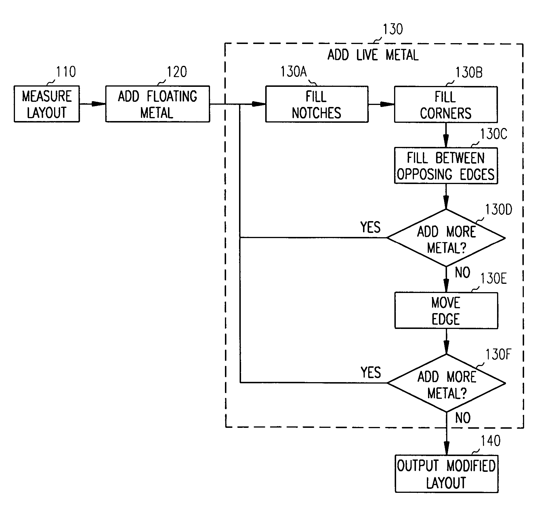
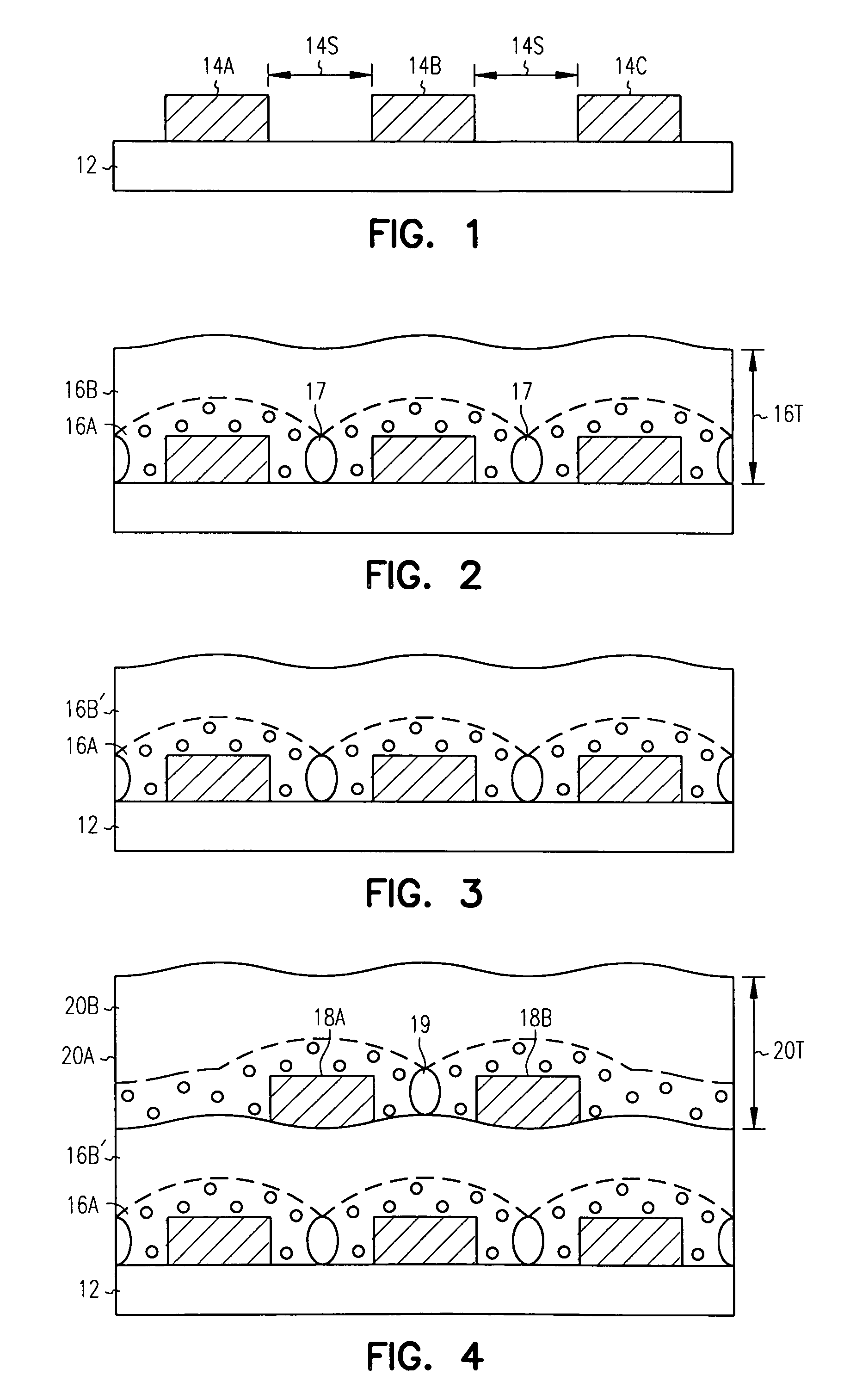
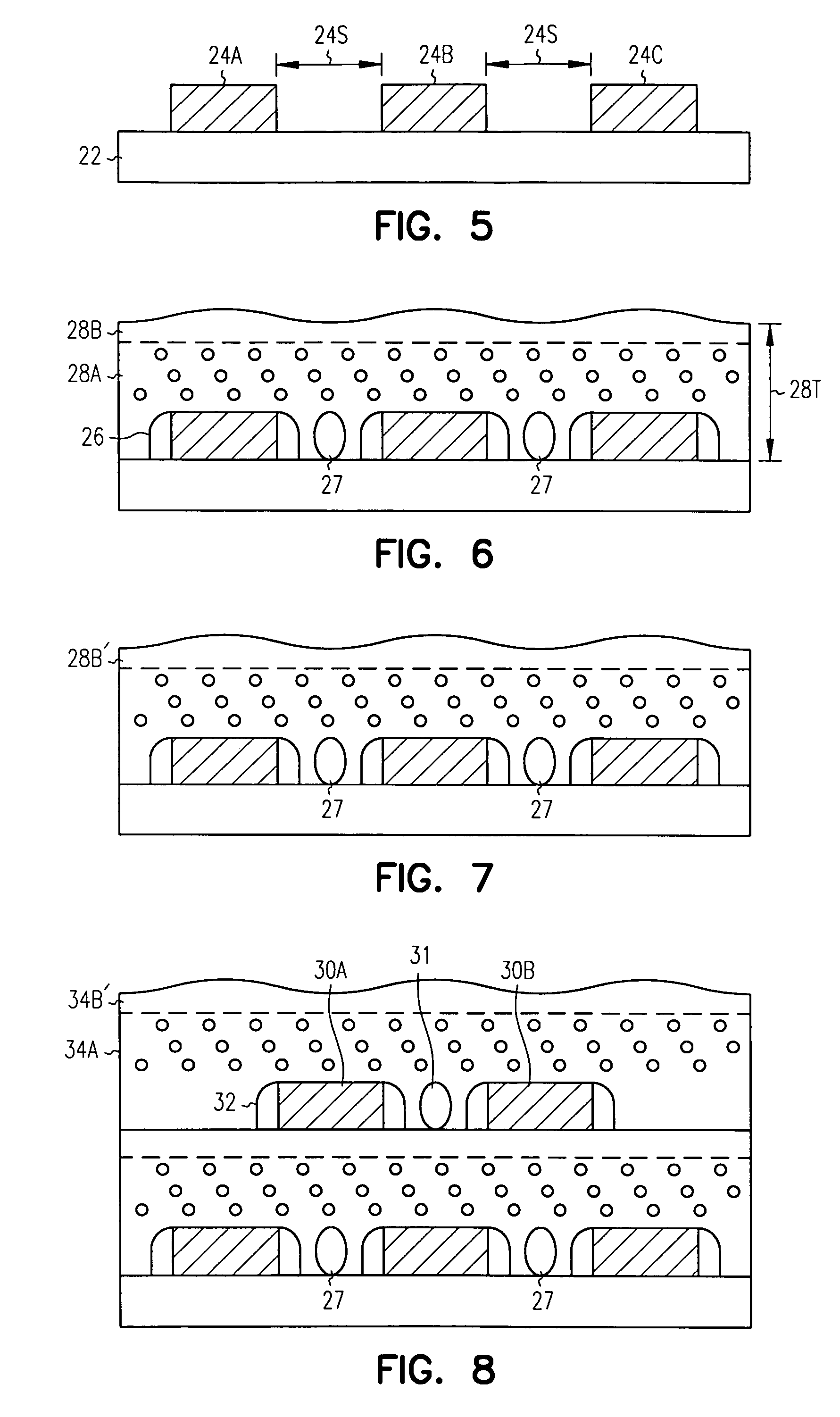
[0030]FIGS. 1-4 show a number of exemplary integrated-circuit assemblies, which taken collectively and sequentially, illustrate an exemplary method of making nearly planar or quasi planar dielectric films, or layers, within the scope of the present invention. As used herein, a quasi planar film is globally planar with local nonplanarities having slopes less than or equal to 45 degrees and depths less than the t...


PUM


Abstract

In the fabrication of integrated circuits, one specific technique for making surfaces flat is chemical-mechanical planarization. However, this technique is quite time consuming and expensive, particularly as applied to the numerous intermetal dielectric layers—the insulative layers sandwiched between layers of metal wiring—in integrated circuits. Accordingly, the inventor devised several methods for making nearly planar intermetal dielectric layers without the use of chemical-mechanical planarization and methods of modifying metal layout patterns to facilitate formation of dielectric layers with more uniform thickness. These methods of modifying metal layouts and making dielectric layers can be used in sequence to yield nearly planar intermetal dielectric layers with more uniform thickness.

Description

RELATED APPLICATIONS [0001] This application is a Divisional of U.S. application Ser. No. 10 / 677,057, filed Sep. 30, 2003, which is a Divisional of U.S. application Ser. No. 09 / 801,265, filed Mar. 7, 2001, now U.S. Pat. No. 6,627,549, which claims priority to U.S. Provisional App. 60 / 187,658, filed on Mar. 7, 2000. This application further relates to U.S. application Ser. No. 10 / 926,471. All of these applications are incorporated herein by reference.TECHNICAL FIELD [0002] The present invention concerns methods of making integrated circuits, particularly methods of making metal masks and dielectric, or insulative, films. BACKGROUND OF THE INVENTION [0003] Integrated circuits, the key components in thousands of electronic and computer products, are interconnected networks of electrical components fabricated on a common foundation, or substrate. Fabricators typically build the circuits layer by layer, using techniques, such as doping, masking, and etching, to form thousands and even mi...

Claims


Application Information

Patent Timeline
Patent Type & Authority Applications(United States)
IPC IPC(8): H01L21/4763H01L29/10H01L23/58H01L21/3205H01L21/3105H01L21/316H01L21/768
CPCH01L21/02126H01L21/022H01L21/02203H01L21/02271H01L21/7684H01L21/31612H01L21/31695H01L21/76819H01L21/7682H01L21/31051H01L21/02164H01L21/3105
Inventor JUENGLING, WERNER
Owner MICRON TECH INC
Features
  • R&D
  • Intellectual Property
  • Life Sciences
  • Materials
  • Tech Scout
  • Unparalleled Data Quality
  • Higher Quality Content
  • 60% Fewer Hallucinations
Learn More