In-plane switching mode liquid crystal display device and method for fabricating the same

a liquid crystal display device and switching mode technology, applied in non-linear optics, instruments, optics, etc., to achieve the effect of improving image quality and improving the aperture ratio of the liquid crystal display devi

Inactive Publication Date: 2006-01-05
LG DISPLAY CO LTD
View PDF6 Cites 60 Cited by
  • Summary
  • Abstract
  • Description
  • Claims
  • Application Information

AI Technical Summary

Benefits of technology

[0014] An object of the present invention is to provide an in-plane switching mode liquid crystal display device and a method for fabricating the same that improve an aperture ratio of the liquid crystal display device.
[0015] Another object of the present invention is to provide an in-plane switching mode liquid crystal display device and a method for fabricating the same capable of improving image quality.
[0017] Another object of the present invention is to provide a method for fabricating an in-plane switching mode liquid crystal display device with a reduction in a signal interference.

Problems solved by technology

However, the IPS-LCD device has the following problems.

Method used


Image

  • In-plane switching mode liquid crystal display device and method for fabricating the same
  • In-plane switching mode liquid crystal display device and method for fabricating the same
  • In-plane switching mode liquid crystal display device and method for fabricating the same

Examples


Embodiment Construction

[0034] Reference will now be made in detail to the preferred embodiments of the present invention, examples of which are illustrated in the accompanying drawings.

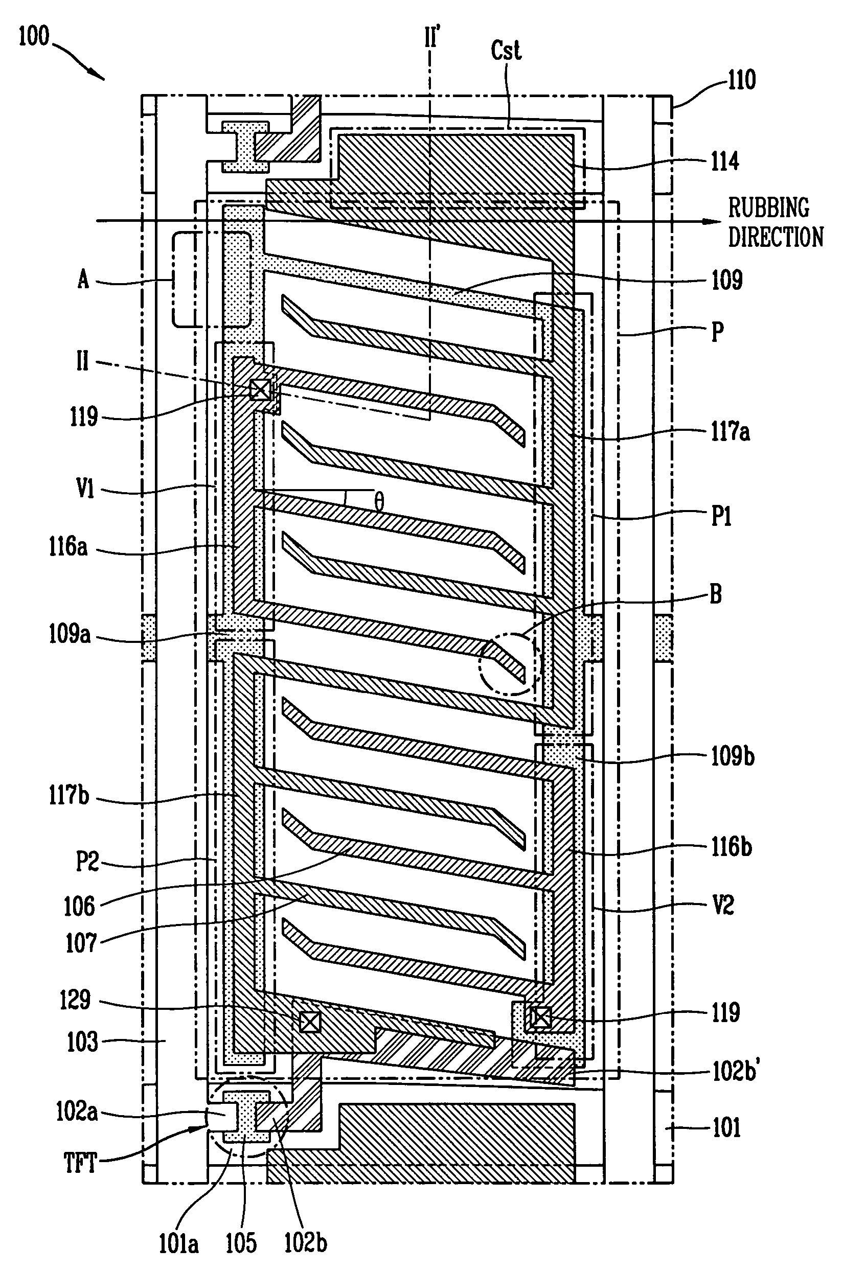
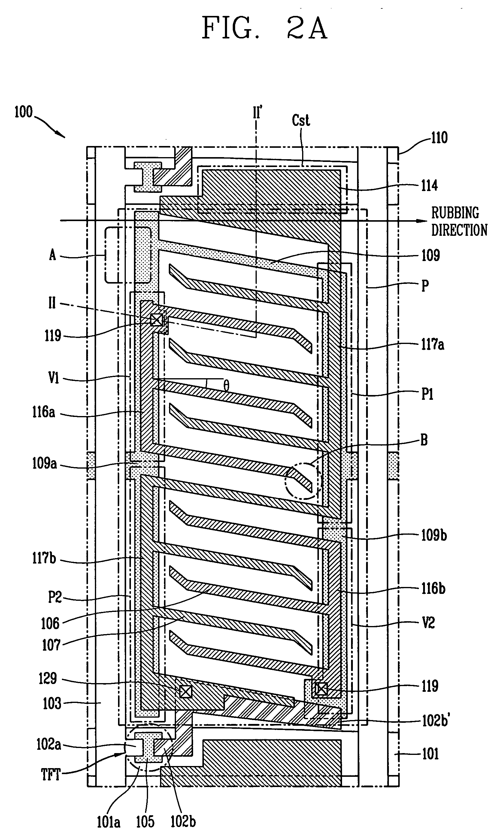
[0035]FIG. 2A is a plane view of an exemplary pixel region according to an embodiment of the present invention. FIG. 2B is a cross-sectional view taken along line II-II′ of FIG. 2A. Referring to FIG. 2A, an IPS-LCD device 100 includes one or more gate line 101 arranged on a transparent first substrate 110 in a first direction and one or more data line 103 arranged in a second direction, and a pixel region (P) is defined a crossing of the one or more gate line 101 and the one or more data line 103. A switching device TFT is formed at the crossing of the gate line 101 and the data line 103. The switching device TFT can be a thin film transistor, which includes a gate electrode 101a, a semiconductor layer 105 formed on the gate electrode 101a, and source and drain electrodes 102a and 102b disposed on the semiconductor layer 1...


PUM

PropertyMeasurementUnit
widthsaaaaaaaaaa
electric fieldaaaaaaaaaa
areaaaaaaaaaaa

Abstract

An in-plane switching mode liquid crystal display device includes a first substrate; a gate line disposed in a first direction on the first substrate; a data line disposed in a second direction on the first substrate, the data line crossing the gate line to define a pixel region; pixel electrodes and common electrodes disposed in the first direction in the pixel region, the pixel electrodes and the common electrodes generating an in-plane electric field within the pixel region; first and second common lines disposed parallel to the data line at right and left sides of the pixel region; a first common electrode connection line connecting at least two common electrodes and forming a first common electrode overlapping region by overlapping the first common line; and a second common electrode connection line connecting at least two other common electrodes and forming a second common electrode overlapping region by overlapping the second common line, wherein the first common electrode overlapping region and the second common electrode overlapping region have substantially the same area.

Description

[0001] This application claims the benefit of Korean Patent Application No. P2004-49777 filed in Korea on Jun. 29, 2004, which is hereby incorporated by reference in its entirety. BACKGROUND OF THE INVENTION [0002] 1. Field of the Invention [0003] The present invention relates to a liquid crystal display device and more particularly, to an in-plane switching mode liquid crystal display device and a method for fabricating the same. [0004] 2. Description of the Related Art [0005] A liquid crystal display (LCD) device is commonly used as a flat panel display device because it provides high quality images and consumes low power. The LCD device is formed by attaching face to face a thin film transistor array substrate and a color filter substrate with a uniform gap between the two substrates, and forming a liquid crystal layer between the two substrates. Pixels are arranged on the thin film transistor array substrate in a matrix. A thin film transistor, a pixel electrode and a capacitor ...

Claims


Application Information

Patent Timeline
Patent Type & Authority Applications(United States)
IPC IPC(8): G02F1/1343
CPCG02F1/134363G02F1/1343
Inventor KIM, DO-SUNGCHOI, WOON-SUB
Owner LG DISPLAY CO LTD
Why Eureka
Try Eureka