
Eureka
For R&D, Eureka makes reading and utilizing patents & technical documents easy.
Eureka AIR
Designed for self-driven R&D workflows. Generate viable solutions, solve complex R&D challenges, empower your innovation with AI.

Eureka Materials
Designed for material experts only. Revolutionize your material R&D, from search, analyze, to developing new materials.

TechResearch
Generate reliable direction feasibility study reports for your R&D in just a few steps.

TechSeek
Discover and master advanced knowledge NOW. Basics, ideas, possibilities, all at once.

TechMind
As an expert in R&D Theories, TechMind can generates customized viable solutions instantly.

TechRisk
Analyze your overall solution with one click, know your potential R&D risks in advance.

TechMonitor
Get weekly tech updates, stay abreast of the latest tech innovations and key insights.
Digital-to-analog converter with secondary resistor string
- Summary
- Abstract
- Description
- Claims
- Application Information
AI Technical Summary
Benefits of technology
Problems solved by technology
Method used
Image

Examples
first embodiment
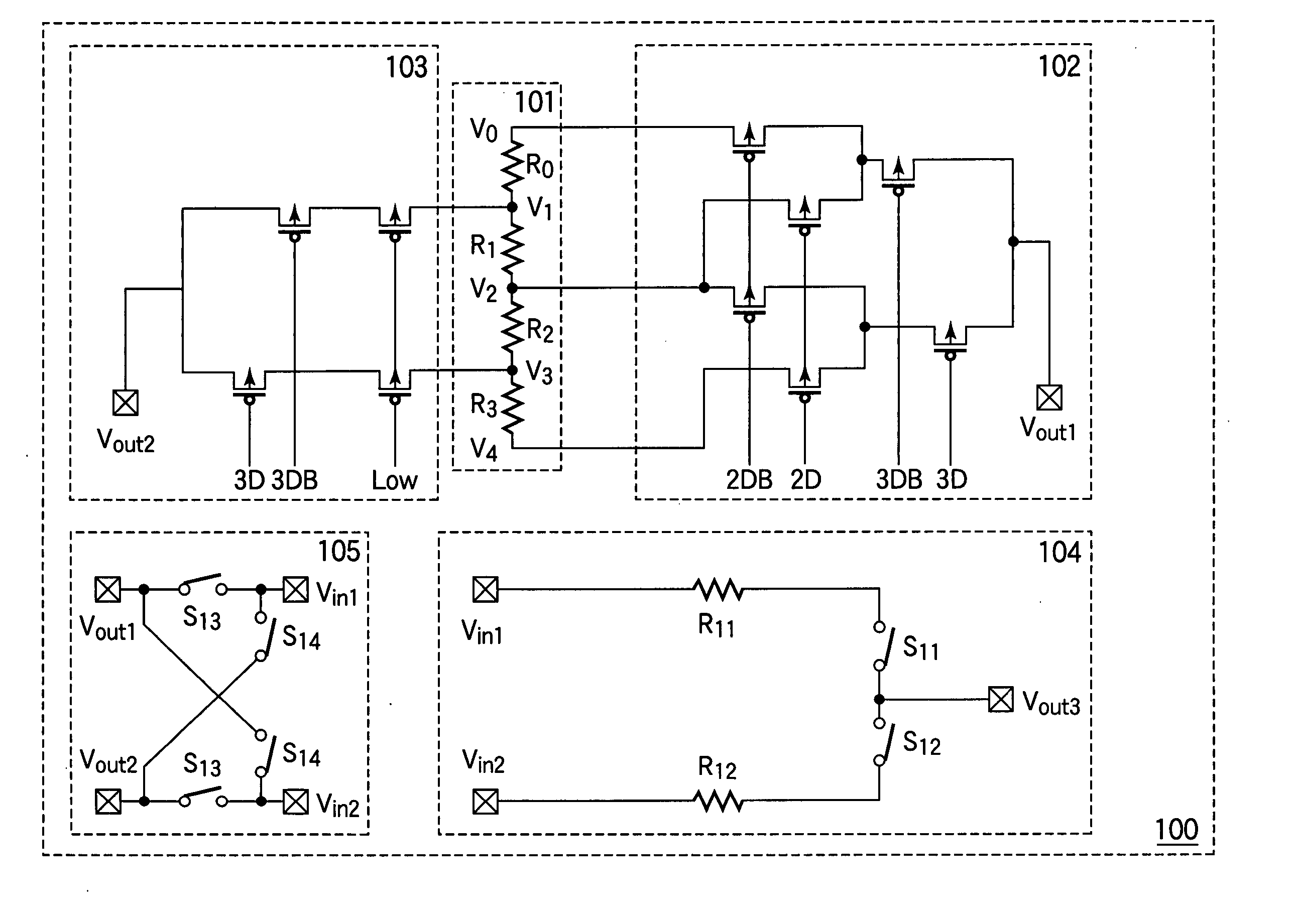
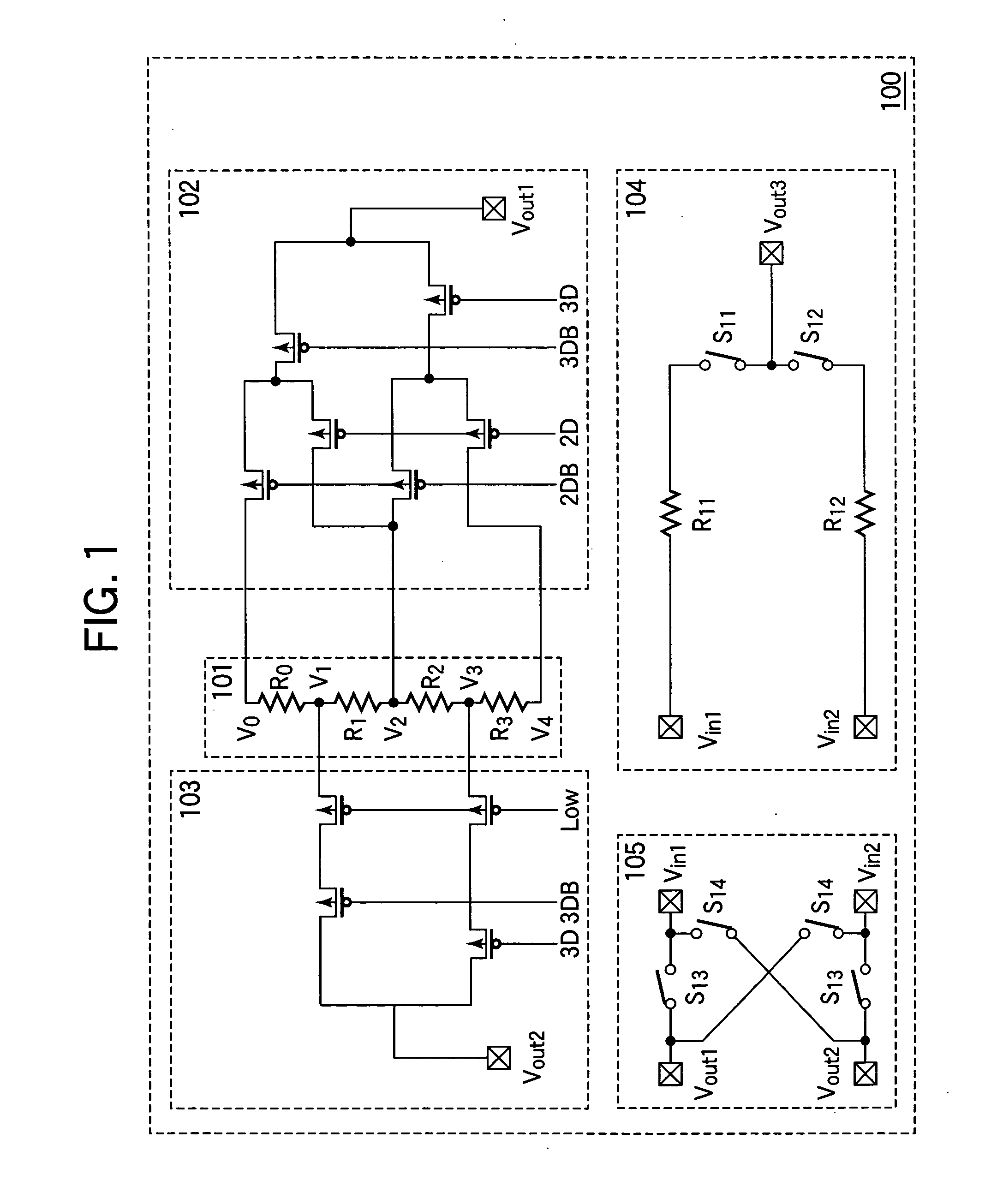
[0017] The first embodiment is a D / A converter that converts n-bit digital data to an analog signal. Referring to FIG. 1, the D / A-converter 100 comprises a voltage generator 101 and three control circuits 102, 103, 104. The illustrated circuit converts three-bit digital data comprising bits 1D, 2D, 3D and their complementary values 1DB, 2DB, 3DB.
[0018] The voltage generator 101 is a string of resistors (R0, R1, R2, R3) connected in series, receiving a voltage V0 from a power source (not shown) and generating successively lower voltages (V1 to V4) by resistive voltage drops. Voltages V0 to V4 will be referred to below as reference voltages. In general, if n is the number of bits of digital input data, the voltage generator 101 in the first embodiment has 2n-1 resistors generating 2n-1+1 reference voltages.
[0019] The first control circuit 102 uses the upper two bits of input data (2D, 3D and their complementary values 2DB and 3DB) to select one of the even-numbered reference voltage...
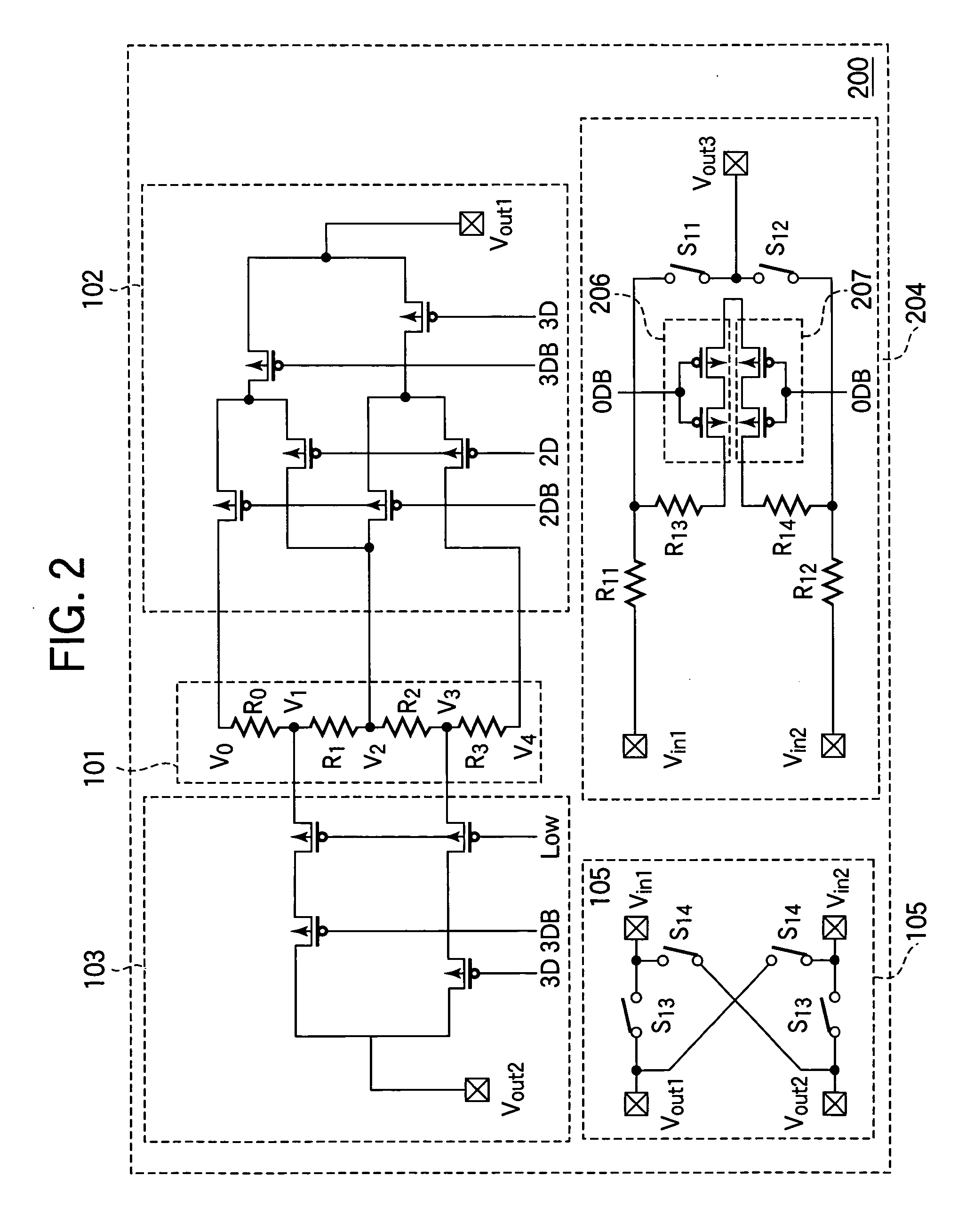
second embodiment
[0042] The second embodiment is a modification of the first embodiment that operates as an (n+1)-bit D / A converter. In the example shown in FIG. 2, the second embodiment is a four-bit D / A converter receiving digital data bits 0D, 1D, 2D, 3D, and their complementary values 0DB, 1DB, 2DB, 3DB. The second embodiment has the same voltage generator 101, first control circuit 102, second control circuit 103, and switching circuit 105 as the first embodiment, but has a modified third control circuit 204, described below.
[0043] As in the first embodiment, the third control circuit 204 connects the first input Vin1to the third output Vout3 through a first resistor R11 and first switch S11, and connects the second input Vin2 to the third output Vout3 through a second resistor R12 and second switch S12. In addition, the third control circuit 204 connects a node disposed between the first resistor R11 and first switch S11 and a node disposed between the second resistor R12 and second switch S1...
PUM
 Abstract
Description
Claims
Application Information
 - R&D Engineer
- R&D Manager
- IP Professional
- Industry Leading Data Capabilities
- Powerful AI technology
- Patent DNA Extraction
Browse by: Latest US Patents, China's latest patents, Technical Efficacy Thesaurus, Application Domain, Technology Topic, Popular Technical Reports.
© 2024 PatSnap. All rights reserved.Legal|Privacy policy|Modern Slavery Act Transparency Statement|Sitemap|About US| Contact US: help@patsnap.com