

Projection optical system, exposure apparatus, and exposure method
a technology which is applied in the field of projection optical system and exposure apparatus, can solve the problems of irregular resolution and unsuitability for lithography, and achieve the effect of large resolution
- Summary
- Abstract
- Description
- Claims
- Application Information
AI Technical Summary
Benefits of technology
Problems solved by technology
Method used
Image

Examples
Embodiment Construction
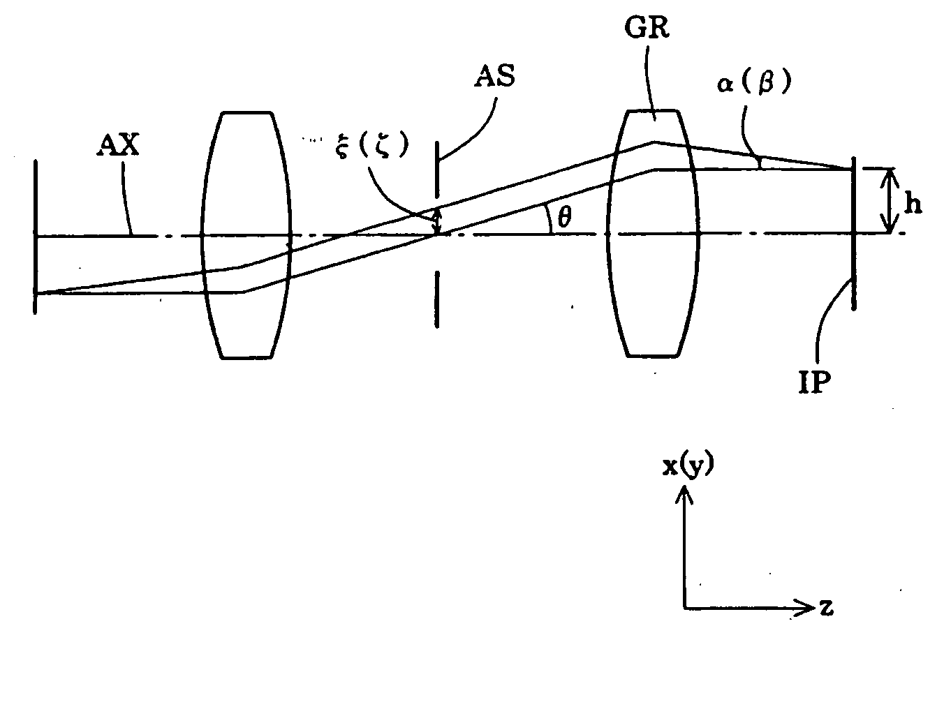
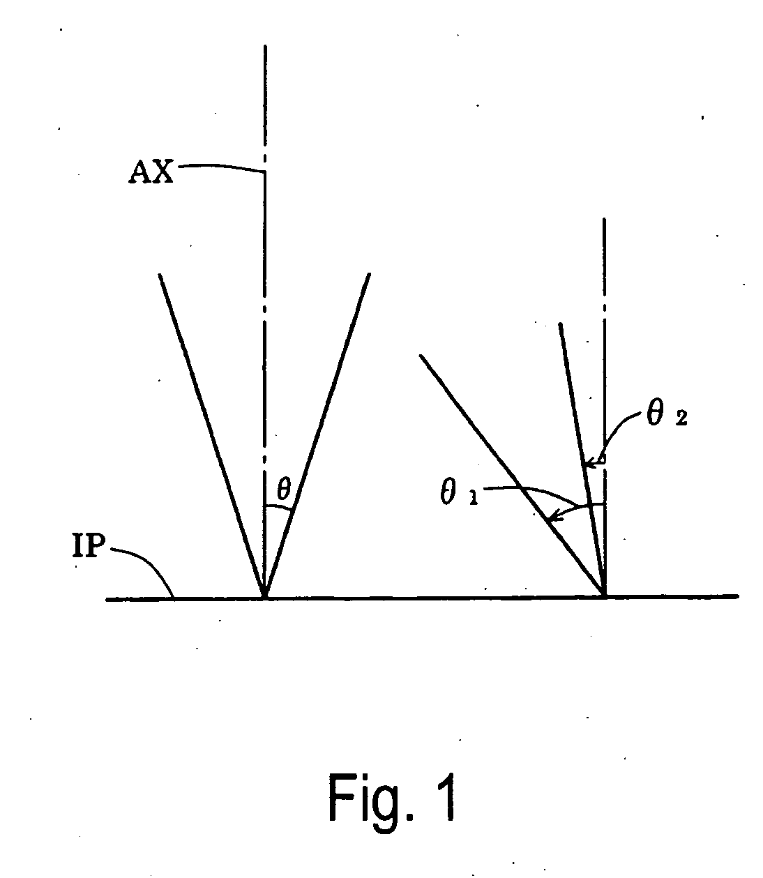
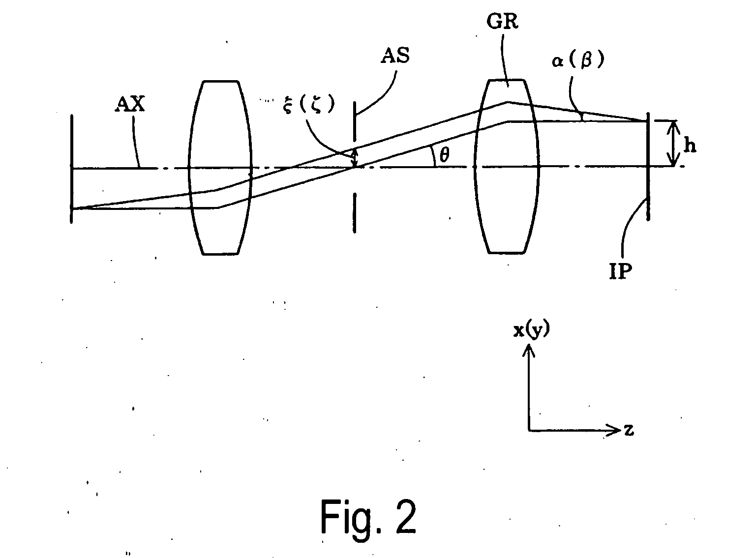
[0030] The following specifically explains problems of conventional technology prior to explaining embodiments of this invention. In a reflective type projection optical system in which a view of field region and an imaging region are positioned apart from an optical axis, a numerical aperture on the optical axis cannot be defined with its usual meaning. Therefore, the numerical aperture NA off the optical axis is defined as shown in FIG. 1.
[0031] In FIG. 1, a numerical aperture NAo on an optical axis is shown by the following equation (1), using an angle that an outermost light beam (light beam reaching an image plane IP passing through a periphery of an aperture portion) reaching the image plane IP forms with an optical axis AX, that is, incident angle θ. Meanwhile, a numerical aperture NA off the optical axis is defined by the following equation (2), using incident angles θ1 and θ2 of the outermost light beams reaching the image plane IP.
NAo=sin θ (1)
NA=(sin θ1−sin θ2) / 2 (2)...
PUM
 Abstract
Description
Claims
Application Information