Integrated circuit probe card

a probe card and integrated circuit technology, applied in the direction of electrical testing, measurement devices, instruments, etc., can solve the problems of inability to individually adjust the contact force applied by each probe on the corresponding pad, inability to measure the electrical properties of the device under test, and abrasion wear, etc., to achieve the effect of easily adjusting the coplanarity

Inactive Publication Date: 2006-02-02
MICROELECTRONICS TECH INC
View PDF18 Cites 19 Cited by
  • Summary
  • Abstract
  • Description
  • Claims
  • Application Information

AI Technical Summary

Benefits of technology

[0013] Compared with prior art, the present integrated circuit probe card rotates the screw contacting the side of the wedge to move the wedge laterally, and the inclined surface of the wedge moves the adjusting pin upwards and downwards to further adjust the coplanarity between the probe assembly and the device under test. The present invention can adjust the coplanarity easily by the wedges with an appropriate inclined surface and screws with an appropriate pitch. In addition, different from the prior art using the vertical movement of differential screws to adjust the coplanarity, the present invention adjusts the coplanarity between the probe assembly and the device under test by the lateral movement of the wedge through the rotation of the screw. Furthermore, the contact force (F) transmitted to the probe by the device under test is transferred to the inclined surface of the wedge, and consequently renders the direction of the friction force (f) generated by the vertical component force (Fv) of the force (F) on the inclined surface, is opposite to that of the horizontal component force (Fh) of the contact force (F). Consequently, a certain magnitude of friction force associated with a coefficient of friction will be generated on the inclined surface, thereafter to counteract the horizontal component force (Fh) and physically lock the lateral position of the adjusting pin automatically, so that the coplanarity between the probe assembly and the device under test will be maintained.

Problems solved by technology

As a result, it is impossible to measure the electrical properties of the device under test 52 accurately.
The probe 42 with a shrunk arrangement tends to be abrasively worn off, it is because of sanding process may introduce a large process variation errors; therefore, the sanding technology for planarizing the tip of the probe 42 cannot be applied to the probe 42 arranged with the shrunk design rule.
However, the disclosure of U.S. Pat. No. 6,586,956 B2 can only fine-adjust the planarity of the probe holder entirely, and the contact force applied by each probe on the corresponding pad cannot be adjusted individually if there is difference between the lengths of the probes.
However, the above-mentioned prior art references are complicated and inconvenient in adjusting the coplanarity between the probe card and the device under test, therefore it is necessary to improve the design of the prior art.

Method used


Image

  • Integrated circuit probe card
  • Integrated circuit probe card
  • Integrated circuit probe card

Examples


first embodiment

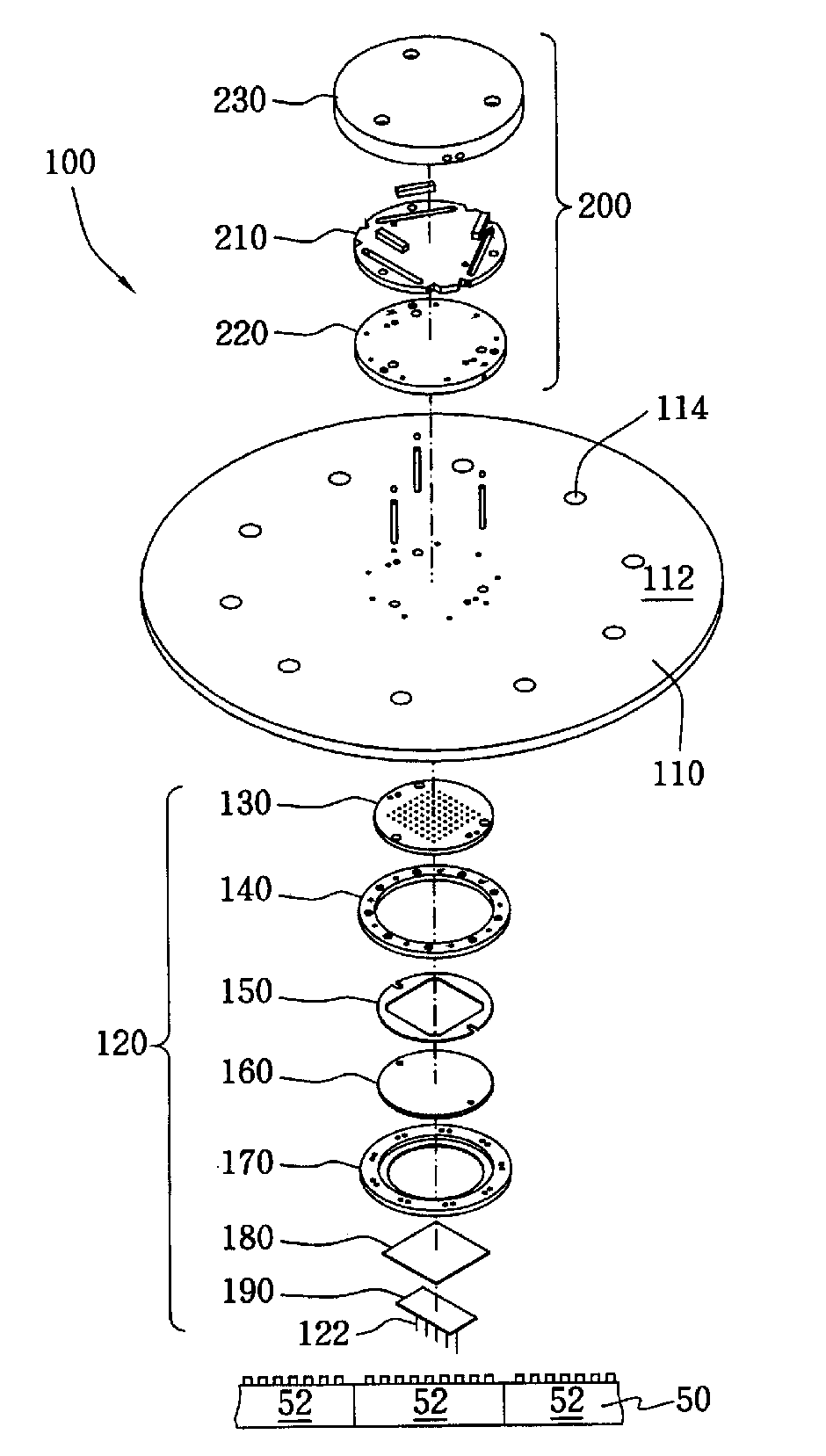
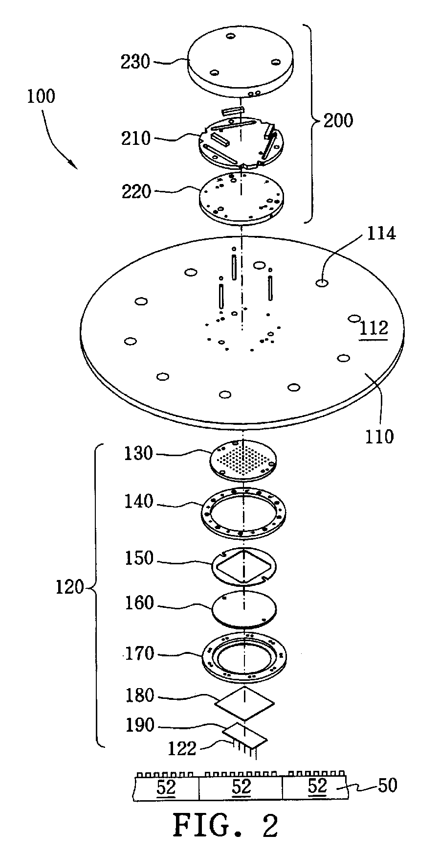
[0026]FIG. 2 illustrates an integrated circuit probe card 100 according to the present invention. As shown in FIG. 2, the integrated circuit probe card 100 comprises a primary circuit board 110, a probe assembly 120 including a plurality of probes 122 and an adjusting assembly 200 for adjusting the coplanarity between the probe assembly 120 and a wafer 50 including several integrated circuit devices 52. The primary circuit board 110 comprises a plurality of testing contacts 114 positioned on the upper surface 112 for electrical connecting a test machine (not shown in FIG. 2). The adjusting assembly 200 comprises an upper cover 230, a groove plate 210 and a guiding plate 220. The probe assembly 120 comprises an elastic connector 130, a spacer 140, a stress dispersion plate 150, an interface circuit board 160, a bottom cover 170, a space transformer 180 and a probe contactor 190.

[0027]FIG. 3 is a cross-sectional view of the probe assembly 120 according to the present invention. As sho...

second embodiment

[0042]FIG. 13 illustrates an integrated circuit probe card 300 according to the present invention. The bottom cover 310 of the integrated circuit probe card 300 also supports the interface circuit board 160, the stress dispersion plate 150 and the elastic connector 130. Compared with the bottom cover 170 fixed onto the spacer 140 directly by the screw 172 as shown in FIG. 8, the bottom cover 310 of the integrated circuit probe 300 shown in FIG. 11 is fixed on the spacer plate 314 via a plurality of spring steels 312, which are further fixed on the spacer plate 314 directly via the screw 318. Since the elasticity of the spring steels 312 can provide an appropriate moving space, the coplanarity between the space transformer 180 and the device under test 52 can be adjusted without releasing the screw 318 in advance.

[0043] Compared with prior art, the present integrated circuit probe card 100 possesses the following advantages:

[0044] Different from the prior art using the vertical move...


PUM


Abstract

The probe card comprises a primary circuit board with a plurality of signal contacts, a probe assembly including a plurality of probes electrically connected to the signal contact and an adjusting assembly for adjusting the coplanarity between the probe assembly and a device under test. The adjusting assembly comprises a groove plate with a plurality of grooves, a wedge positioned in the groove, at least one adjusting pin connecting the wedge and the probe assembly and at least one screw positioned at one side of the wedge. The wedge comprises an inclined surface, and one end of the adjusting pin contacts the inclined surface of the wedge and the other end contacts the probe assembly. The circuit probe card moves the wedge laterally to further move the adjusting pin upwards and downwards, so that to the coplanarity between the probe assembly and the device under test can be adjusted.

Description

BACKGROUND OF THE INVENTION [0001] (A) Field of the Invention [0002] The present invention relates to an integrated circuit probe card with a planarity adjusting mechanism, and more particularly to an integrated circuit probe card with a planarity adjusting mechanism capable of adjusting the coplanarity between an integrated circuit device under test and a probe assembly including several probes. [0003] (B) Description of the Related Art [0004] Generally, it is necessary to test the electrical characteristic of integrated circuit devices on the wafer level for checking whether the integrated circuit device satisfies the product specification. Integrated circuit device with electrical characteristic satisfying the specification will be selected to carry on the subsequent packaging process, and other devices will be discarded to avoid additional packaging cost. Another electrical property test will be performed on the integrated circuit device after the packaging process is completed ...

Claims


Application Information

Patent Timeline
Patent Type & Authority Applications(United States)
IPC IPC(8): G01R31/02
CPCG01R1/07342
Inventor FAN, HORNG-KUANGSUDIN, HENDRA
Owner MICROELECTRONICS TECH INC
Why Eureka
Try Eureka