Defect monitor for semiconductor manufacturing capable of performing analog resistance measurements

a defect monitor and semiconductor technology, applied in the field of semiconductor manufacturing, can solve problems such as structure under test failure and structure under test failur

Inactive Publication Date: 2006-02-02
IBM CORP
View PDF1 Cites 10 Cited by
  • Summary
  • Abstract
  • Description
  • Claims
  • Application Information

AI Technical Summary

Benefits of technology

[0008] In another preferred embodiment, a test structure is provided in which a first structure under test is connected to a test short line and a second structure under test is connected through a transistor to ground, wherein a critical spacing exists between the first test structure and the second test structure. The test short line carries a signal that indicates whether the critical spacing is shorted. If the critical spacing is shorted, then the structures under test fail.
[0009]

Problems solved by technology

If the structure under test is open, then the structure under test fails

Method used


Image

  • Defect monitor for semiconductor manufacturing capable of performing analog resistance measurements
  • Defect monitor for semiconductor manufacturing capable of performing analog resistance measurements
  • Defect monitor for semiconductor manufacturing capable of performing analog resistance measurements

Examples


Embodiment Construction

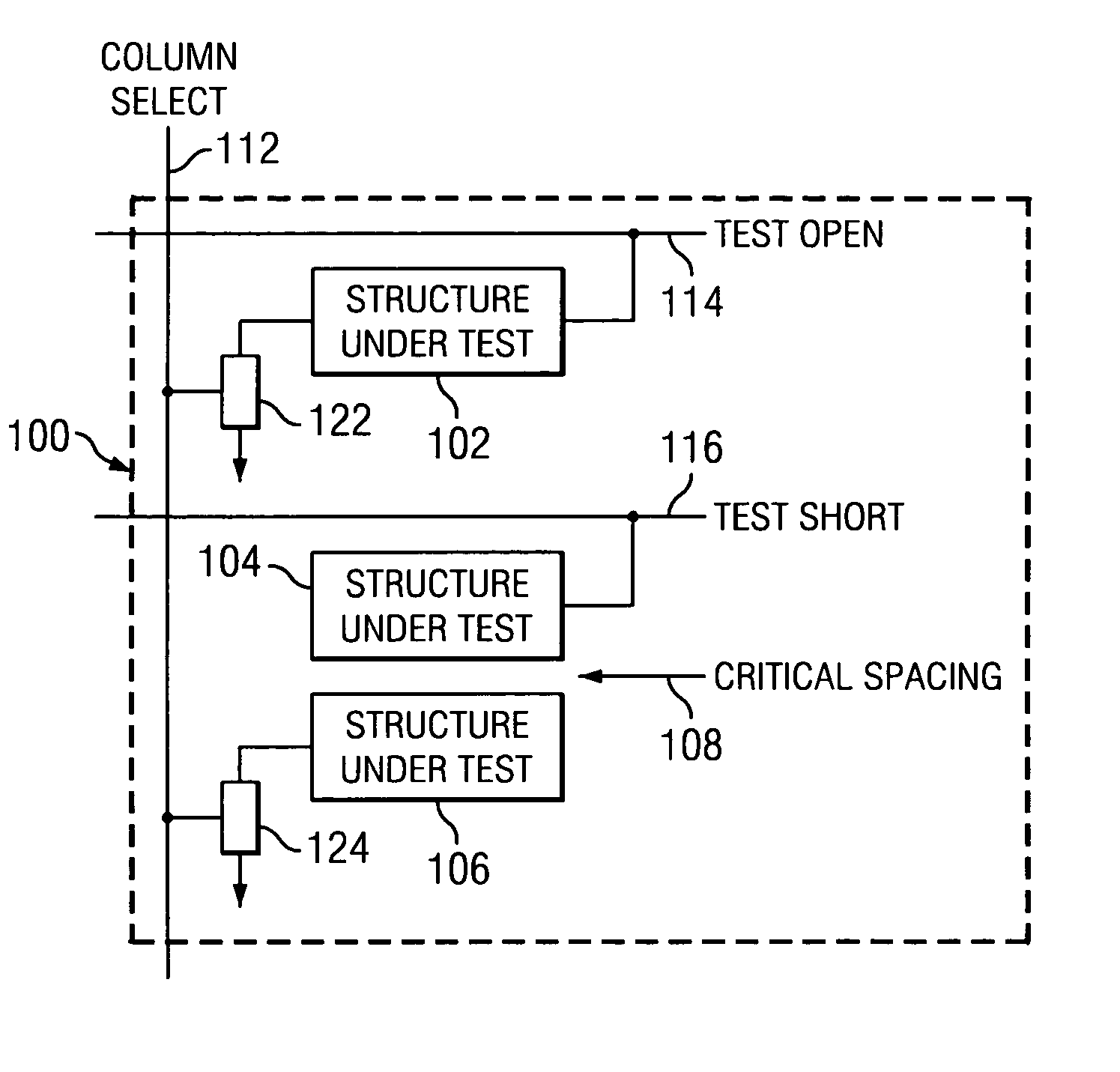
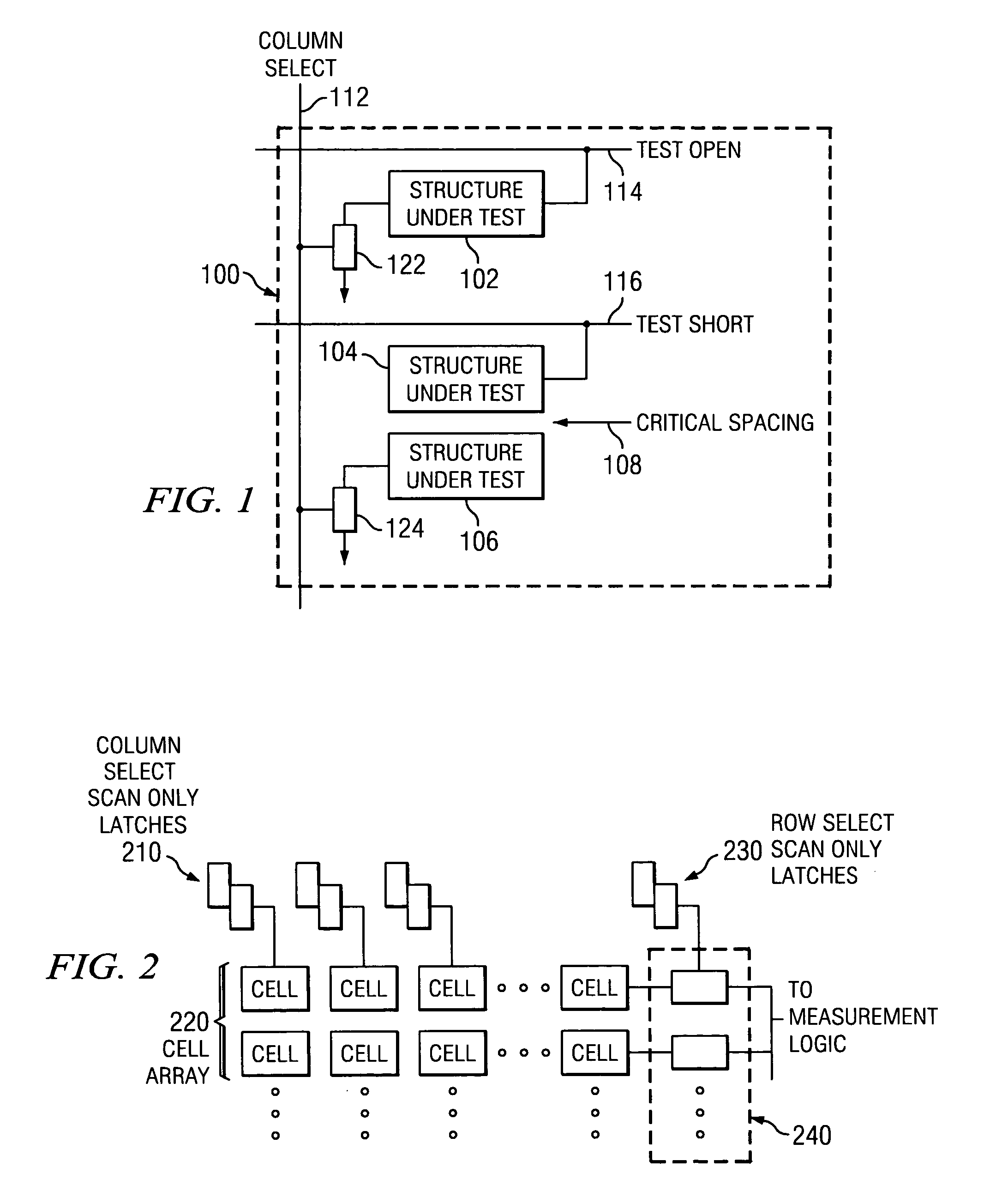
[0017] With reference now to the figures, FIG. 1 depicts a pictorial representation of a cell in a test structure in accordance with an exemplary embodiment of the present invention. Cell 100 is a semiconductor device that includes structures under test 102, 104, 106. More particularly, structure under test 102 may be a long wire or via chain, for example. Wires may appear in metal layers or in the semiconductor. Cell 100 may be one of many semiconductor devices on a chip. A chip may have ten or more metal layers. Vias are used to connect metal layers to other metal layers or to portions of the semiconductor. Cell 100 is a test structure that is designed to isolate structures under test 102, 104, 106 and critical spacing 108 to determine whether structure under test 102 is defective.

[0018] Structure under test 102 is connected to test open line 114. Structure under test 102 is also connected through transistor 122 to ground. Transistor 122 may be, for example, an N-type field effec...


PUM


Abstract

A mechanism is provided to address a structure under test and to identify a point of failure. A test open line carries a signal that indicates whether a structure under test is open or closed. A test short line carries a signal that indicates whether a structure under test is shorted. A test structure may include an array of cells, where each cell includes a circuit including structures to test. The cells may be scanned using scan only latches and signals on the test open and/or test short lines may be recorded. A test circuit may include a digital mode and an analog mode. The digital mode provides an open or closed value. The analog mode includes a programmable load. The output of the analog mode provides a resistance value that is relative to the programmable load.

Description

BACKGROUND OF THE INVENTION [0001] 1. Technical Field [0002] The present invention relates to semiconductor manufacturing and, in particular, to testing of semiconductor devices. Still more particularly, the present invention provides a defect monitor for semiconductor manufacturing capable of performing analog resistance measurements. [0003] 2. Description of Related Art [0004] Bringing up a new semiconductor can be challenging and requires a variety of yield monitors to determine the health of the process and to find systematic problems. Several known structures, such as long wires, minimum spaced wires, and via chains are used to determine back end of line health. Back end of line (BEOL) includes wires and vias. Front end of line (FEOL) includes transistors and other devices. Wires may appear in metal layers or in the semiconductor itself. Vias are used to connect metal layers to other metal layers or to portions of the semiconductor device. [0005] When a long wire is fabricated,...

Claims


Application Information

Patent Timeline
IPC IPC(8): G01R31/26G01R31/50
CPCG01R31/024G01R31/50
Inventor BARISH, ARNOLD E.JAMES, NORMAN KARL
Owner IBM CORP
Why Eureka
Try Eureka