
Accurate density calculation with density views in layout databases

a layout database and accurate density technology, applied in the field of calculating density for integrated circuit design, can solve the problems of inaccurate density calculation, inaccurate density calculation, inaccurate density calculation, etc., and achieve the effect of accurately calculating the density of hierarchical blocks

Active Publication Date: 2006-02-02
BELL SEMICON LLC
View PDF6 Cites 25 Cited by
  • Summary
  • Abstract
  • Description
  • Claims
  • Application Information

AI Technical Summary

Benefits of technology

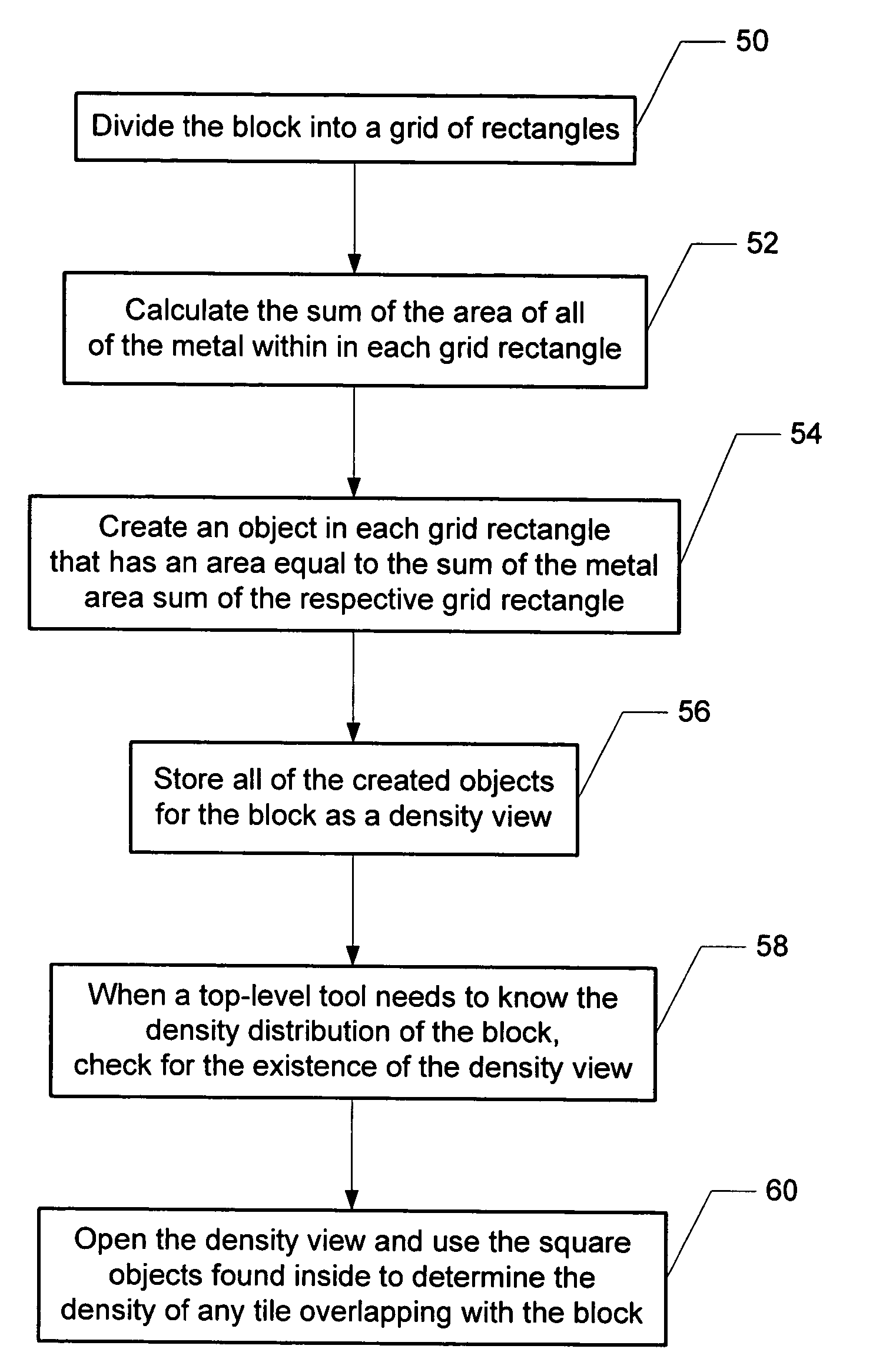
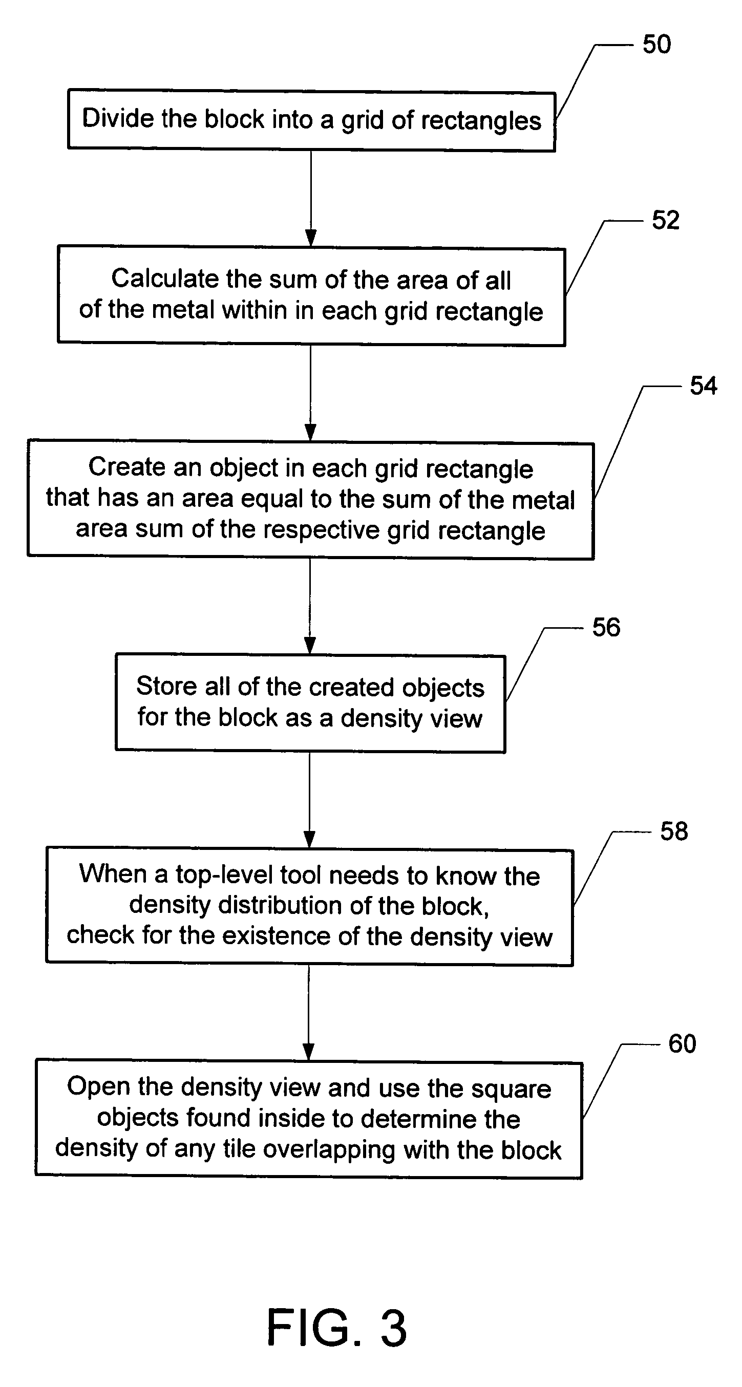
"The present invention provides a method for accurately calculating the density of hierarchical blocks in an integrated circuit design. This is done by creating a density abstraction view for each block, which is a grid of rectangles containing the metal area of each block. The density view is efficient and accurate, as it directly corresponds to the metal distribution in the block. This method is faster and more accurate than using the layout view, and can be stored in a layout database for easy reference."

Problems solved by technology

Most designs today, however, are hierarchical in nature and accurate calculation of density becomes a problem.
In hierarchical designs, accurate calculation of density becomes a problem.
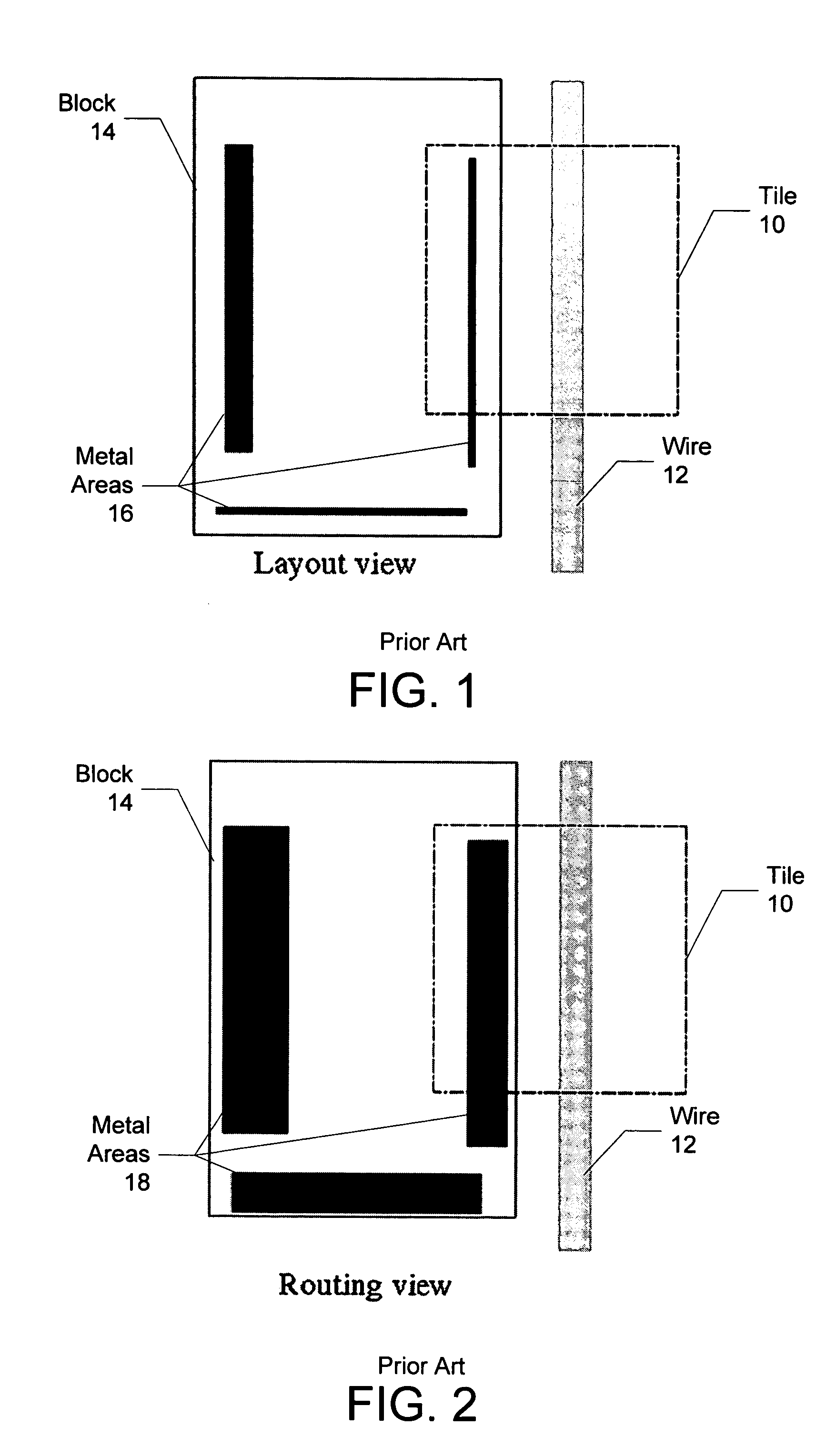
As a result, metal area sum calculations that use routing abstractions tend to overestimate density and are inaccurate.
Also, the large number and complicated geometries of objects in the routing abstraction slow down density computation.
Using the original layout view of the block 15 as in FIG. 1, results in accurate density calculations, but at too high a cost of run-time to be a feasible solution due to all the area calculations required for the many individual metal objects.

Method used


Image

  • Accurate density calculation with density views in layout databases
  • Accurate density calculation with density views in layout databases
  • Accurate density calculation with density views in layout databases

Examples


Embodiment Construction

[0018] The present invention relates to calculating density for hierarchical blocks in a circuit design. The following description is presented to enable one of ordinary skill in the art to make and use the invention and is provided in the context of a patent application and its requirements. Various modifications to the preferred embodiments and the generic principles and features described herein will be readily apparent to those skilled in the art. Thus, the present invention is not intended to be limited to the embodiments shown, but is to be accorded the widest scope consistent with the principles and features described herein.

[0019] The present invention provides a method for calculating density of hierarchical blocks in an integrated circuit design by abstracting the density of the hierarchical block into a new view, referred to herein as a density view, that captures the density distribution of the block. Once the density view is created for a hierarchical block, the view i...


PUM


Abstract

Generating a density abstraction view for an integrated circuit design by dividing each block in the design that is larger than a predetermined size into a grid of rectangles; calculating a sum of metal area in each rectangle in the grid; creating an object in each rectangle having an area equal to the metal area sum of the rectangle; and storing all the created objects for the block as a view. The view may be stored in a layout database along with any other views for the integrated circuit design, and then used to determine density of a tile overlapping with the block by adding the area of the square objects in the density view that overlap with the tile to the tile.

Description

FIELD OF THE INVENTION [0001] The present invention relates to calculating density for integrated circuit design, and more particularly to a method for accurately calculating density for the design using an abstracted density view. BACKGROUND OF THE INVENTION [0002] Modern chip fabrication techniques impose restrictions on the density of conductors on a chip. These restrictions are usually implemented as design rules that define square “tiles” of a certain size and minimum and maximum allowable densities for those tiles. The density of a tile is the summation of the area of all metal objects in the tile divided by the area of the tile. A chip design must meet these before it can be taped out and sent to fabrication. [0003] The size of the tile defined by the design rules have rapidly been getting smaller at each technology node, falling at an accelerated rate; much faster than the minimum feature size of objects in the tile. The minimum density rules are checked for and met by metal...

Claims


Application Information

Patent Timeline
Patent Type & Authority Applications(United States)
IPC IPC(8): G06F17/50
CPCG06F17/5081G06F30/398
Inventor SHROWTY, VIKRAMRAMAN, SANTHANAKRISHNAN
Owner BELL SEMICON LLC
Learn More