Display device and driving method thereof

a technology of a display device and a driving method, which is applied in the direction of electric digital data processing, instruments, computing, etc., can solve the problems of inability to accommodate the required number of pixels, inconvenient use of these structures, and inability to meet the requirements of pixels, so as to reduce the number of elements per pixel and improve image quality

Active Publication Date: 2006-02-09
SHARP KK
View PDF43 Cites 21 Cited by
  • Summary
  • Abstract
  • Description
  • Claims
  • Application Information

AI Technical Summary

Benefits of technology

[0030] The present invention, in view of the problems, has an objective to provide a display device and its driving method for better image quality. The invention achieves this by reducing element counts per pixel, hence pixel size (by even a small amount), to cram more pixels in a predetermined screen size.

Problems solved by technology

Inconveniences may however occur with these structures.
A required number of pixels may not be accommodated in a predetermined screen size.
These problems can occur even with a top emission structure where emitted light is let out from the sealing film, opposite the TFT substrate.
A required number of pixels may not be accommodated in a predetermined screen size.
These problems can occur, again, even with a top emission structure.

Method used


Image

  • Display device and driving method thereof
  • Display device and driving method thereof
  • Display device and driving method thereof

Examples


embodiment 1

[0092] Present embodiment 1 will describe a first example of the display device in accordance with the present invention.

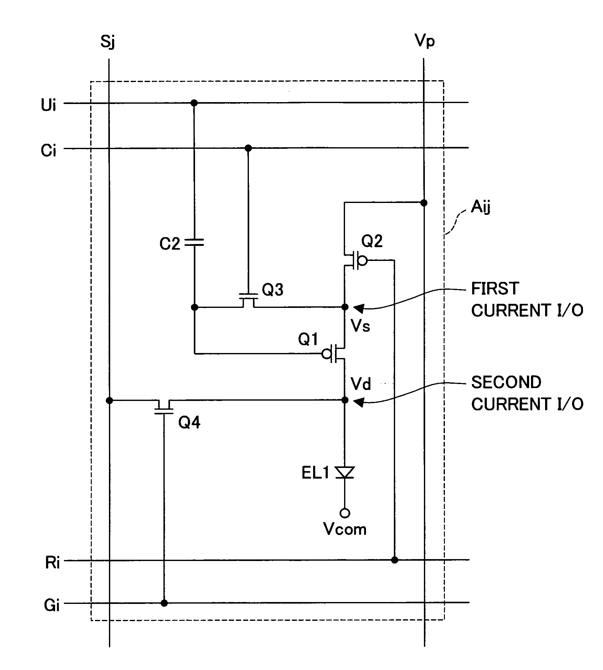
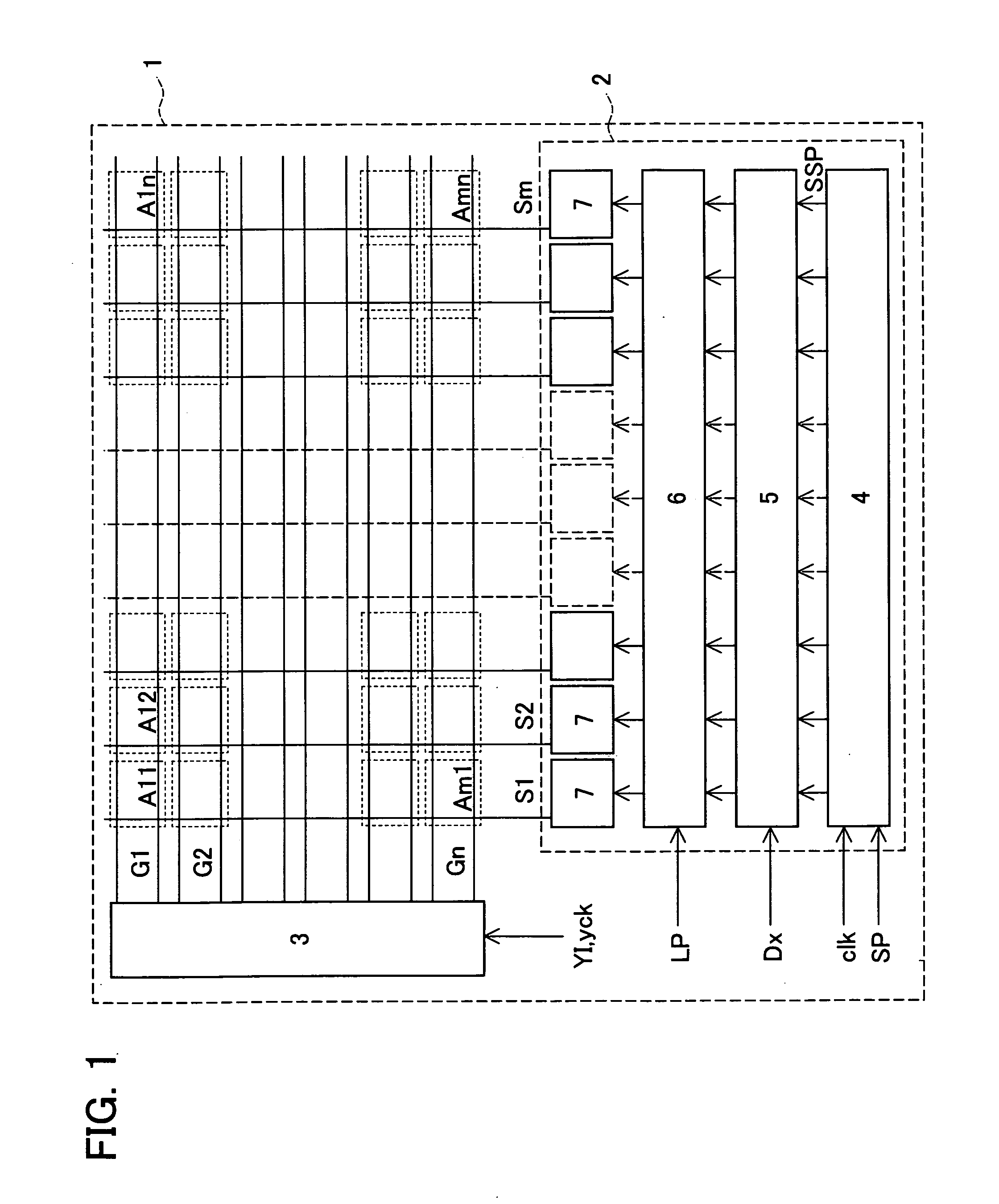
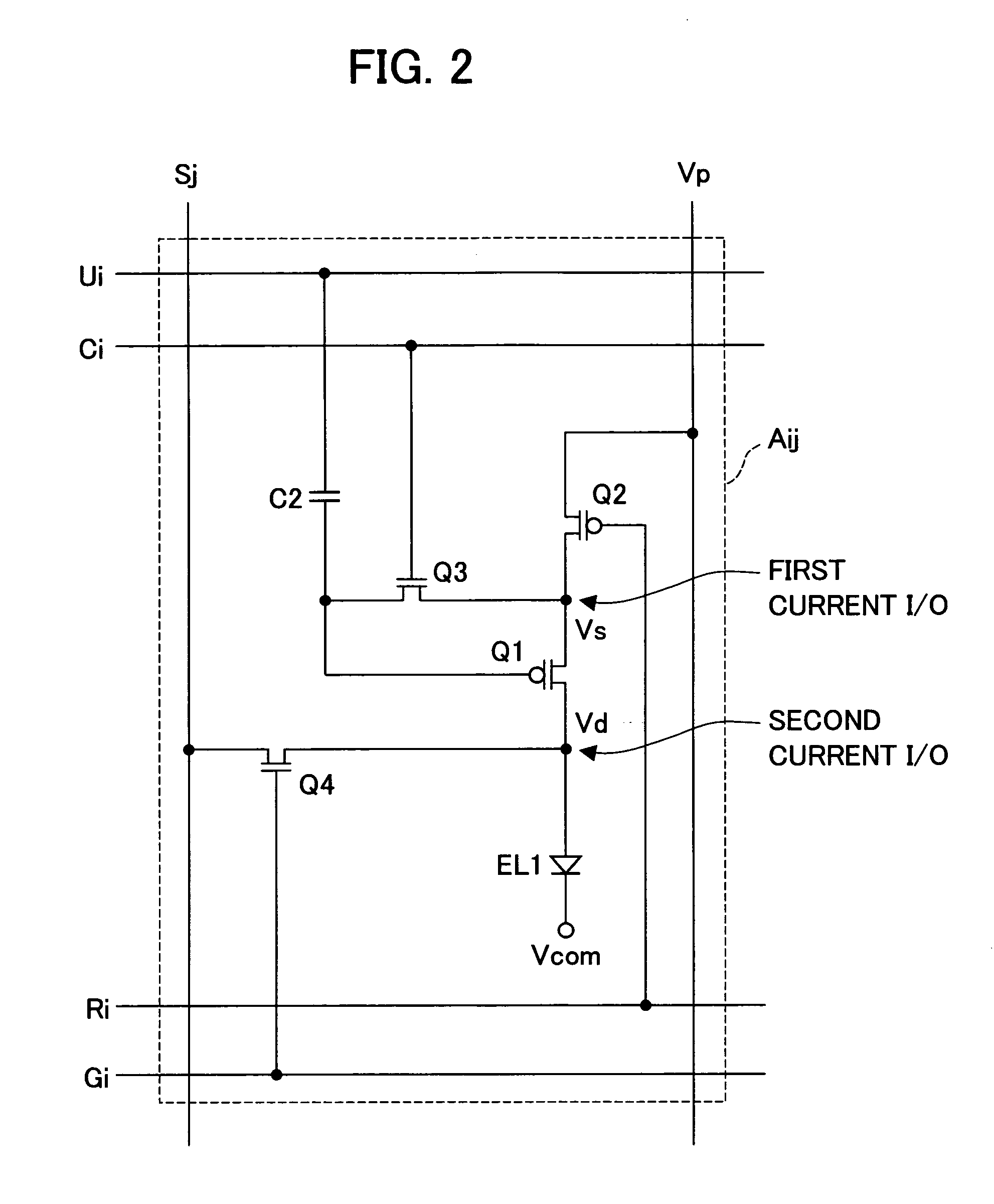
[0093] As shown in FIG. 1, a display device 1 of the present embodiment has pixel circuits Aij, a gate driver circuit 3, and a source driver circuit 2. The circuits Aij are arranged in a matrix. The circuits 2, 3 control the lines.

[0094] Each pixel circuit Aij is located at an intersection of a source line Sj and a gate line Gi (i and j are integers). The source driver circuit 2 has an m-bit shift register 4, a 6 m-bit register 5, a 6 m-bit latch 6, and m 6-bit D / A converter circuits 7.

[0095] As such, in the source driver circuit 2, a start pulse SP is fed to the first register in the m-bit shift register 4 and transferred through the shift register 4 in accordance with a clock clk. Concurrently, the start pulse SP is also supplied to the register 5 as timing pulses SSP. The 6 m-bit register 5 holds 6-bit data Dx for the source lines Sj at the timing pulses SSP...

embodiment 2

[0129] Present embodiment 2 will describe a second example of the display device in accordance with the present invention. The display device 1 of the present embodiment is the same as the display device 1 shown in FIG. 1; its description is not repeated here. FIG. 8 shows a pixel circuit structure in accordance with the present invention for present embodiment 2.

[0130] The illustrated pixel circuit Aij has a gate line Gi replacing and acting as both the control line Ri and gate line Gi in FIG. 2. The control line Ri was connected to the gate of the switching TFT Q2 (first switching transistor). The gate line Gi was connected to the gate of the switching TFT Q4 (third switching transistor). Otherwise, the pixel circuit Aij is identical to the FIG. 2 pixel circuit; no more description will be given here.

[0131] Now, the operation of the pixel circuit Aij will be described in reference to the a timing chart of FIG. 9.

[0132]FIG. 9 shows timings indicated by voltages on 1) the electri...

embodiment 3

[0143] Present embodiment 3 will describe a third example of the display device in accordance with the present invention. As shown in FIG. 13, a display device 10 of the present embodiment has pixel circuits Aij, a gate driver circuit 3, and a source driver circuit 8. The pixel circuits Aij are arranged in a matrix. The circuits 3, 8 control the lines. The FIG. 1 structure may be used in this embodiment. Conversely, the FIG. 13 structure may be used in other embodiments.

[0144] Each pixel circuit Aij is located at an intersection of a source line Sj and a gate line Gi. The source driver circuit 8 has an m-bit shift register 4 and m sample and hold circuits 9.

[0145] As such, in the source driver circuit 8, a start pulse SP is fed to the first register in the m-bit shift register 4 and transferred through the shift register 4 in accordance with a clock clk. The start pulse SP is supplied to the sample and hold circuits 9 as timing pulses SSP. The sample and hold circuits 9 acquire an...


PUM


Abstract

A display device in accordance with the present invention changes to Vc the voltage of a terminal of a capacitor C2 the other terminal of which is connected to the gate of a driver TFT Q1. Thus, a desired voltage Vda is fed from a source line Sj to the drain of the driver TFT Q1 so as to adjust the threshold voltage Vth of the driver TFT Q1. The device then changes the voltage of the terminal of the capacitor C2 to Va to render the gate voltage of the driver TFT Q1 Vda−Vth−Vc+Va. A power supply voltage Vp is fed from the source of the driver TFT Q1. Controlling the voltages Vda enables the specification of the output current value of the driver TFT Q1 regardless of its threshold voltage Vth.

Description

[0001] This Nonprovisional application claims priority under 35 U.S.C. § 119(a) on Patent Application No. 2004-229854 filed in Japan on Aug. 5, 2004, the entire contents of which are hereby incorporated by reference. FIELD OF THE INVENTION [0002] The present invention relates to display devices and driving methods for OLED (organic light-emitting diode) displays, FEDs (field emission displays), and other current-driven devices. BACKGROUND OF THE INVENTION [0003] Recent years have seen many research and development activities to manufacture OLED displays, FEDs, and other current-driven light-emitting devices. Especially, the OLED display is the focus of attention in view of possible applications in mobile phones, PDAs (personal digital assistants), and like mobile devices, to exploit its low voltage / low power consumption. [0004]FIG. 39 shows the circuit structure of an OLED pixel disclosed in Published Japanese Translation of PCT Application 2002-514320 (Tokuhyo 2002-514320; publishe...

Claims


Application Information

Patent Timeline
Patent Type & Authority Applications(United States)
IPC IPC(8): G09G3/30
CPCG09G3/3233G09G2300/0417G09G2300/0814G09G2310/027G09G2300/0842G09G2300/0861G09G2300/0819
Inventor NUMAO, TAKAJI
Owner SHARP KK
Why Eureka
Try Eureka