Liquid crystal display

a liquid crystal display and display technology, applied in the direction of identification means, instruments, optics, etc., can solve the problems of affecting the visual appearance of the portion of the display, affecting the human eye, and affecting the effect of lighting leakage, so as to prevent the effect of light leakag

Active Publication Date: 2006-02-09
SAMSUNG DISPLAY CO LTD
View PDF7 Cites 22 Cited by
  • Summary
  • Abstract
  • Description
  • Claims
  • Application Information

AI Technical Summary

Benefits of technology

[0022] In the above structure, possible light leakage can be prevented

Problems solved by technology

As the brightness at the first gate line portion is usually brighter compared to other gate line portions, the picture images displayed at that portion disturbs the human eye.
However, when the G0 line is connected to the G2 line, the integrated circuit (IC) for d

Method used


Image

  • Liquid crystal display
  • Liquid crystal display
  • Liquid crystal display

Examples


Embodiment Construction

[0041] Preferred embodiments of this invention will be explained with reference to the accompanying drawings.

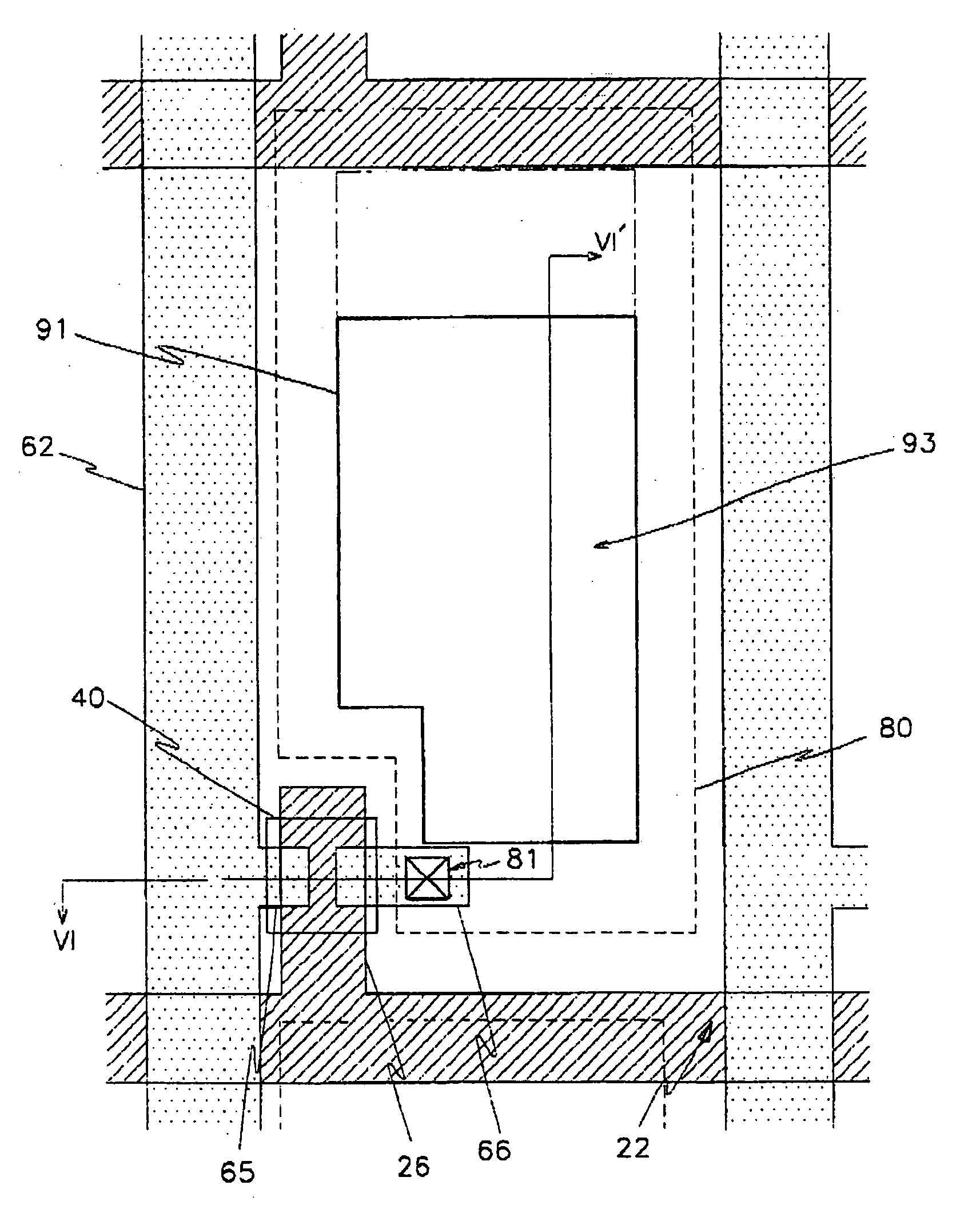
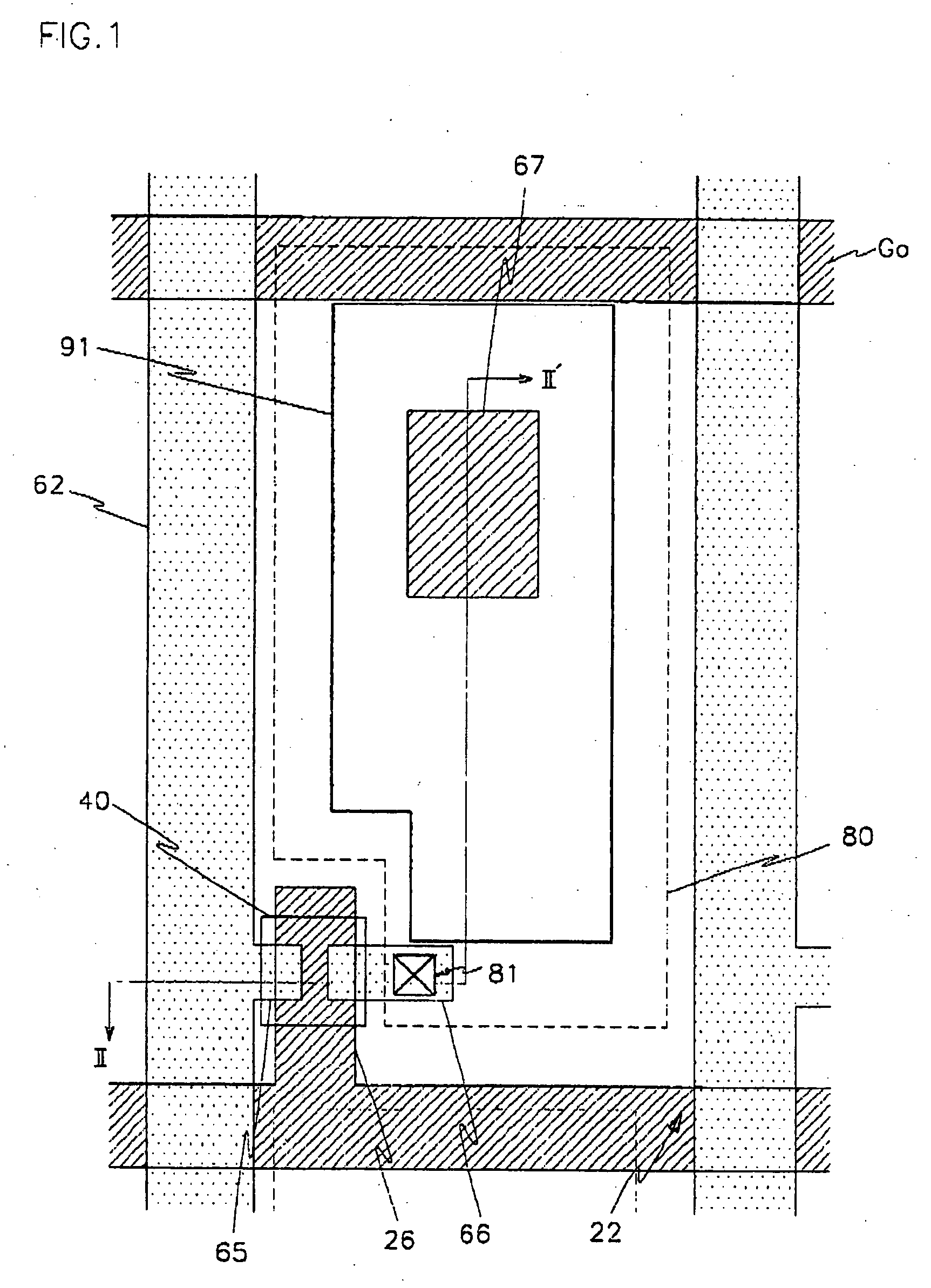
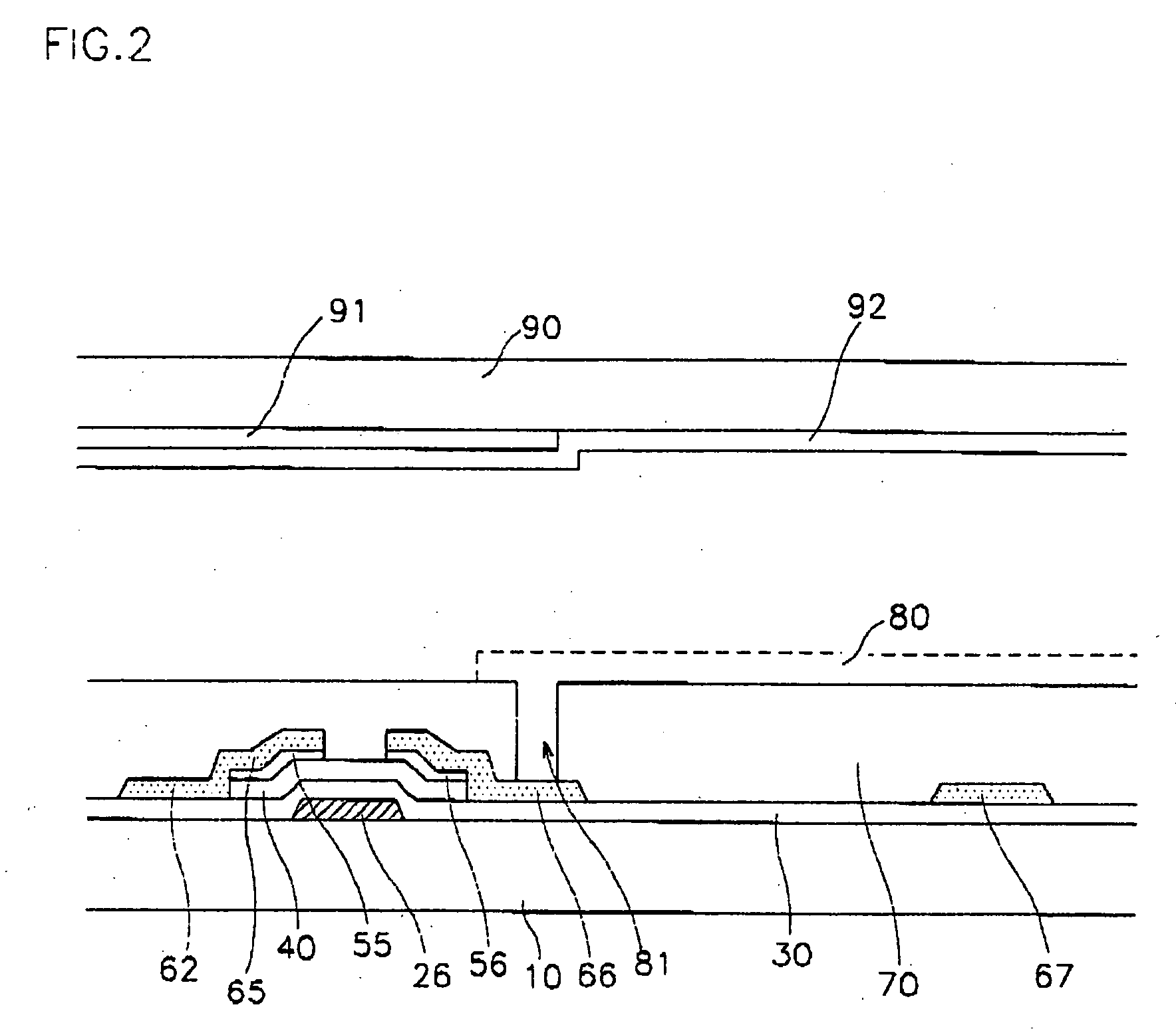
[0042]FIG. 1 is a plan view of a liquid crystal display according to a first preferred embodiment of the present invention where one pixel area of the first pixel row is illustrated, and FIG. 2 is a cross sectional view of the liquid crystal display taken along the II-II′ line of FIG. 2. The liquid crystal display according to the present invention has a basic structure where a liquid crystal layer is sandwiched between upper and lower substrates with a plurality of pixel areas at different pixel rows, and the following description will be made with respect to one pixel area at the first pixel row.

[0043] As shown in the drawings, the lower substrate 10 is overlaid with a first gate line 22 proceeding in the horizontal direction, a gate electrode 26 branched perpendicularly from the first gate line 22 and a storage capacitor line G0 proceeding parallel to the first gate line...


PUM


Abstract

A liquid crystal display includes first and second insulating substrates facing to each other, and a liquid crystal sandwiched between the first and second substrates. A plurality of gate lines are formed at the first substrate to transmit scanning signals, and data lines cross over the gate lines to transmit picture signals. Pads are connected to the gate and data lines. Pixels are demarcated by the gate lines and the data lines, and collectively form a display area. The gate lines demarcate the pixels into rows, and the data lines demarcate the pixels into columns. A black matrix defines each pixel, and a pixel electrode is formed at the pixel. A storage capacitor line is formed at the first substrate parallel to the gate line, and overlapped with the pixel electrodes at the first pixel row. Storage capacitors are formed between the pixel electrodes and the previous gate lines as well as between the pixel electrodes and the storage capacitor line. A gate-off voltage or a common electrode voltage is applied to the storage capacitor line. The opening ratio of each pixel at the first pixel row with the storage capacitor formed between the corresponding pixel electrode and the storage capacitor line differs from the opening ratio of the pixels at the other pixel rows. The difference in the opening ratio is made through forming a light interception pattern at each pixel of the first pixel row, or through differentiating opening areas of the black matrix. In order to prevent leakage of light, light interception patterns may be formed at the region between the display area and the pads.

Description

BACKGROUND OF THE INVENTION [0001] (a) Field of the Invention [0002] The present invention relates to a liquid crystal display and, more particularly, to a liquid crystal display which bears uniform brightness characteristic over the entire screen area without leakage of light. [0003] (b) Description of the Related Art [0004] Generally, a liquid crystal display has an upper substrate with a common electrode and color filters (usually called the “color filter substrate”), a lower substrate with thin film transistors and pixel electrodes (usually called the “TFT array substrate”), and a liquid crystal layer sandwiched between the color filter substrate and the TFT array substrate. Different electrical potentials are applied to the pixel electrodes and the common electrode while forming electric fields to change the liquid crystal molecule orientation. In this way, the light transmission is controlled to display picture images. [0005] In such a liquid crystal display, with only a TFT a...

Claims


Application Information

Patent Timeline
IPC IPC(8): G02F1/1343G02F1/136G02F1/00G02F1/1335G02F1/1362G02F1/1368G09F9/00G09F9/30
CPCG02F1/133512G02F1/136209G02F2001/136218G02F2201/40G02F1/136213G02F1/136218
Inventor KIM, DONG-GYU
Owner SAMSUNG DISPLAY CO LTD
Why Eureka
Try Eureka