Opto-electrical module for optical signals from at least two optical data channels for arranging on a main circuit board of a component assembly and opto-electrical component assembly

a technology of opto-electrical modules and optical signals, which is applied in the direction of optics, instruments, optical light guides, etc., can solve the problems of difficult realization of use in a transceiver module of sff or sfp design, inability to arrange on a central part of the module, and inability to achieve the opto-electronic performance of such bidirectional main circuit boards. achieve the effect of simple and cost-effective design

Active Publication Date: 2006-02-09
II VI DELAWARE INC
View PDF13 Cites 9 Cited by
  • Summary
  • Abstract
  • Description
  • Claims
  • Application Information

AI Technical Summary

Benefits of technology

[0020] The unlocking barrier is advantageously supported on an optical plug pushed into the receptacle, in order thus to prevent unlocking when the plug has been inserted.
[0021] In this case, the locking lever is preferably elastic and comprises an engagement region, which is arranged on the locking lever and can be moved with the latter, for engagement into an engagement opening of the assembly. For the simple and cost-effective design of the unlocking barrier, the latter is advantageously arranged on that side of the locking lever which is opposite to the engagement region.

Problems solved by technology

However, the optoelectronic performance of such bidirectional main circuit boards is not outstanding.
What is disadvantageous about this arrangement is that use in a transceiver module of SFF or SFP design is difficult to realize.
In particular, the small tube with the optical waveguide cannot be arranged centrally in the module for space reasons.

Method used


Image

  • Opto-electrical module for optical signals from at least two optical data channels for arranging on a main circuit board of a component assembly and opto-electrical component assembly
  • Opto-electrical module for optical signals from at least two optical data channels for arranging on a main circuit board of a component assembly and opto-electrical component assembly
  • Opto-electrical module for optical signals from at least two optical data channels for arranging on a main circuit board of a component assembly and opto-electrical component assembly

Examples


Embodiment Construction

[0036] In the following description of the figures, the same reference symbols are used for the same structural parts throughout the figures.

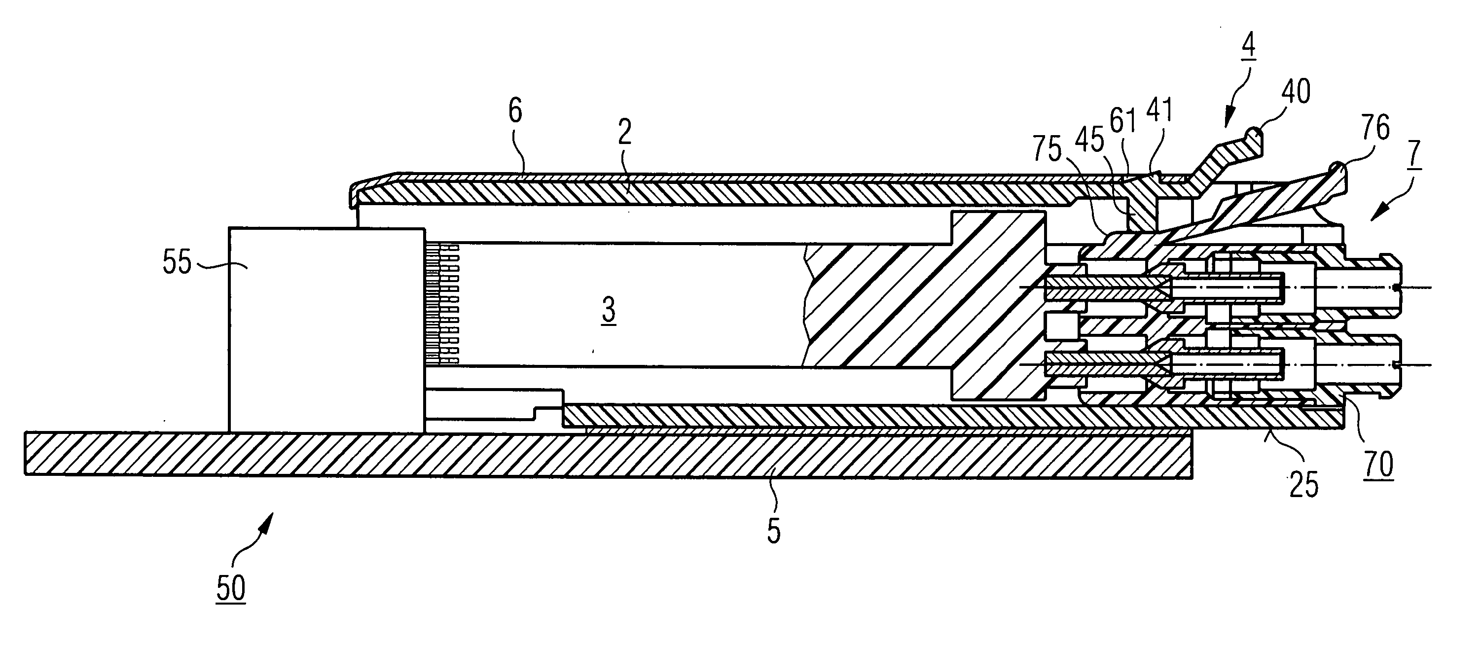
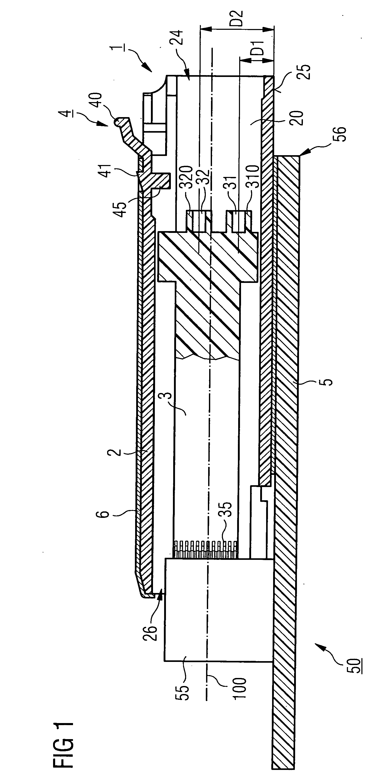
[0037]FIG. 1 shows a sectional illustration of an optoelectronic module 1 arranged on a main circuit board 5 of an assembly 50 of an optical communication system. In this case, the main circuit board 5 of the assembly 50 of the optical communication system is advantageously arranged in, a rack cabinet (not illustrated here), the edge 56 of the main circuit board 5 pointing in the direction of the end side of the rack cabinet from which the assembly 50 is accessible.

[0038] The optoelectronic module 1 has a housing 2 having an underside 25, the underside 25 serving for the arrangement of the housing 2 or the optoelectronic module 1 on the main circuit board 5 of the assembly 50. In this case, the underside 25 of the housing 2 is in contact with the main circuit board 5 directly or indirectly, for example by arrangement on an intermediate elemen...


PUM


Abstract

The invention relates to an optoelectronic module for optical signals of two optical data channels for arrangement on a main circuit board of an assembly, having a housing, which has an underside for arrangement of the optoelectronic module on a main circuit board. The arrangement further includes a printed circuit board arranged in the housing, having a first optical coupling region and a second optical coupling region for the coupling of optical waveguides, wherein the first and second coupling regions are arranged on the printed circuit board. The first optical coupling region is arranged at a smaller distance from the underside of the housing than the second optical coupling region. The invention achieves an efficient utilization of the end area of an assembly.

Description

BACKGROUND OF THE INVENTION [0001] In optical communication technology, large volumes of data are transmitted in complex networks, optoelectronic modules for a plurality of optical channels being used within a system. In particular, optoelectronic modules equipped with a transmission channel and a reception channel, so-called transceivers, are used for this purpose. [0002] So-called small form factor (SFF) transceivers and small form factor pluggable (SFP) transceivers of small design are known. The transceivers may be of pluggable design (SFP transceivers) or be fixedly arranged in a housing on a main circuit board of an assembly of an optical communication system (SFF transceivers). The advantage of pluggable transceivers is that they can subsequently be inserted into a system and be exchanged simply and the system can thus be adapted simply to the respective stipulations of the optical network. [0003] The known transceivers have, in addition to an optoelectronic transmission modu...

Claims


Application Information

Patent Timeline
Patent Type & Authority Applications(United States)
IPC IPC(8): G02B6/36
CPCG02B6/3897G02B6/4292G02B6/4201
Inventor GUNTHER, PETER UWEKROPP, JORG-REINHARDT
Owner II VI DELAWARE INC
Why Eureka
Try Eureka