Band-gap circuit

a band-gap circuit and circuit technology, applied in the direction of electric variable regulation, process and machine control, instruments, etc., can solve the problems of deterioration of noise and reference voltage variation amount, increase of number of elements as a whole, and worse psrr and noise characteristics, etc., to achieve low noise, low noise, and low psrr

Inactive Publication Date: 2006-02-23
ASAHI KASEI ELECTRONICS CO LTD
View PDF13 Cites 23 Cited by
  • Summary
  • Abstract
  • Description
  • Claims
  • Application Information

AI Technical Summary

Benefits of technology

[0009] Furthermore, it is possible to render current ratios of the first and second voltage control current sources different so as to render ratios of the currents passing through the first and second bipolar transistors different.
[0010] It is possible, by preparing such a band-gap circuit, to provide the band-gap circuit operable at the low supply voltage and having high PSRR, low noise and few voltage variations.

Problems solved by technology

Therefore, there is a problem that the PSRR and noise characteristic are worse than a typical 1.2 V output band-gap circuit.
In addition, there are a large number of current paths, and so the number of elements as a whole increases and the noise and reference voltage variation amounts deteriorate.

Method used


Image

  • Band-gap circuit
  • Band-gap circuit
  • Band-gap circuit

Examples


Embodiment Construction

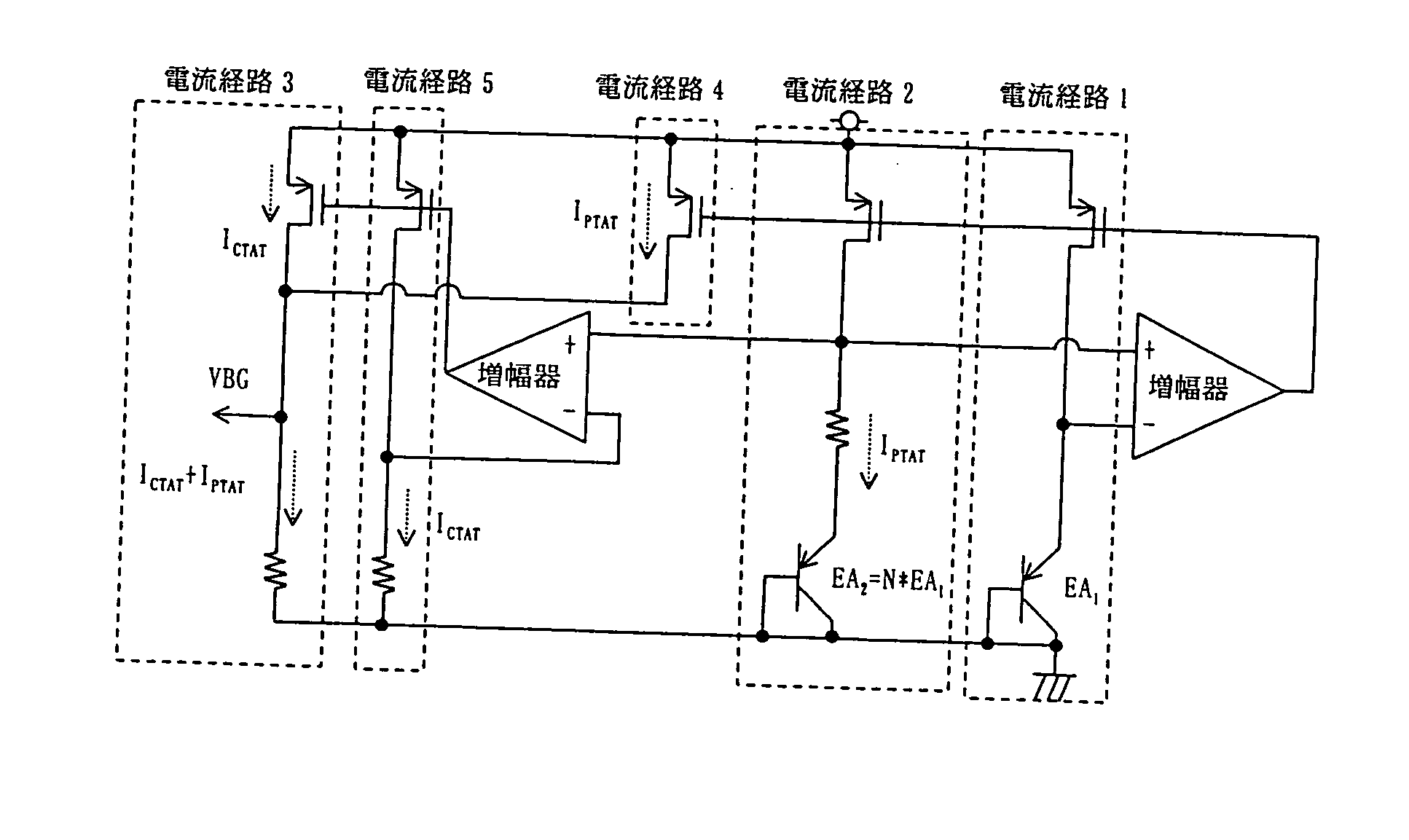
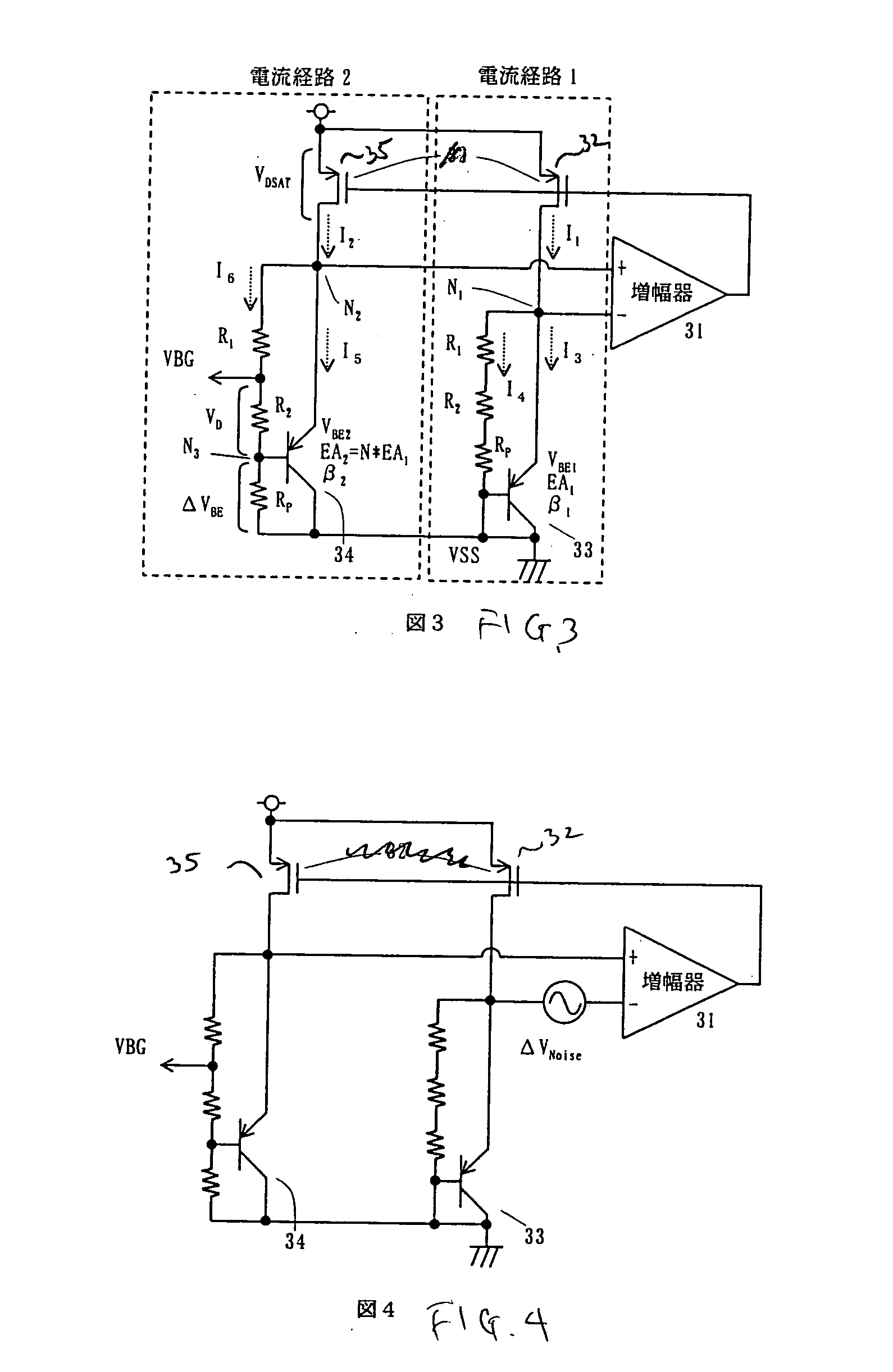
[0016]FIG. 3 is a diagram showing a band-gap circuit according to the present invention, where a current path 1 and a current path 2 are provided between a supply voltage and a ground voltage. The current path 1 is comprised of a PMOS transistor 32 and a bipolar transistor 33, where a source of the PMOS transistor 32 is connected to the supply voltage and a drain of the PMOS transistor 32 is connected to an emitter of the bipolar transistor 33. A collector and a base of the bipolar transistor 33 are connected to a ground potential. Furthermore, a resistor R1, a resistor R2 and a resistor Rp are connected in series between the emitter and base of the bipolar transistor 33.

[0017] The current path 2 is comprised of a PMOS transistor 35 and a bipolar transistor 34, where the source of the PMOS transistor 35 is connected to the supply voltage and the drain of the PMOS transistor 35 is connected to the emitter of the bipolar transistor 34. The collector of the bipolar transistor 34 is co...


PUM


Abstract

A band-gap circuit is constituted by comprising a feedback control amplifier 31 and MOS transistors 32 and 35, having two transistors 33 and 34 of which emitter area is different, comprising resistors R1, R2 and Rp between a base and an emitter of the transistor 33 of which emitter area is smaller, having the resistor Rp between the base and a collector and comprising the resistors R1 and R2 between the base and emitter of the transistor 34 of which emitter area is larger. It is possible to provide the band-gap circuit operable at a low supply voltage and having high PSRR, low noise and few variations.

Description

FIELD OF THE INVENTION [0001] The present invention relates to a band-gap circuit for generating and outputting a reference voltage, and in particular, to the band-gap circuit of high PSRR, low noise and few voltage variations which outputs the reference voltage of a low voltage proportional to a band-gap voltage and having no temperature dependence so as to allow low supply voltage operation. BACKGROUND OF THE INVENTION [0002] Conventionally, a band-gap circuit has been known as a circuit for generating a reference voltage having no temperature dependence. The band-gap voltage generated by the band-gap circuit is 1.2V or so under normal circumstances. However, Japanese Patent Application Laid-Open No. 2002-318626 discloses the band-gap circuit of 0.5V or so as the band-gap circuit operable at low supply voltage. As shown in FIG. 1, it creates, in different circuit blocks, a PTAT (Proportional To Absolute Temperature) current having a characteristic proportional to an absolute tempe...

Claims


Application Information

Patent Timeline
Patent Type & Authority Applications(United States)
IPC IPC(8): G05F1/10
CPCG05F3/30
Inventor OZAWA, KATSUMI
Owner ASAHI KASEI ELECTRONICS CO LTD
Why Eureka
Try Eureka