Methods for minimizing defects when transferring a semiconductor useful layer

a technology of useful layer and defect reduction, which is applied in the direction of semiconductor devices, electrical equipment, basic electric elements, etc., can solve the problems of defects that can detrimentally affect the structural properties of the transfer layer, affecting the efficiency and quality of the bond, and thus the quality of the desired final structure, etc., and achieve the effect of minimizing defects

Inactive Publication Date: 2006-02-23
S O I TEC SILICON ON INSULATOR THECHNOLOGIES
View PDF1 Cites 16 Cited by
  • Summary
  • Abstract
  • Description
  • Claims
  • Application Information

AI Technical Summary

Benefits of technology

[0008] Presented is an advantageous method for minimizing defects when transferring a useful layer from a donor wafer to a receptor wafer is described. The method includes providing a donor wafer having a surface below which a zone of weakness is present to define a useful layer to be transferred, molecularly bonding at a bonding interface the surface of the useful layer of the donor wafer to a surface of the receptor wafer to form a structure, heating the structure at a first temperature that is substantially higher than ambient temperature for a first time period sufficient to liberate water molecules from the bonding interface, with the heating being insufficient to cause detachment of the useful layer at the zone of weakness, and detaching the useful layer from the donor wafer.

Problems solved by technology

A problem associated with such a layer transfer process is that organic or inorganic contaminants or gas pockets may become trapped at the interface of the two wafers during bonding, which can detrimentally affect the efficiency and quality of the bond and thus the quality of the desired final structure.
This problem is of particular concern when one or more additional treatments is / are carried out close to the bonding interface in order to modify the mechanical, physical, or chemical properties of the two wafers.
In particular, such problems may occur when atomic species implantation is conducted close to a wafer surface prior to bonding to form the zone of weakness (for example, when using a “SMART-CUT®” method).
Under these circumstances, contaminants or gas pockets may cause superficial blisters on the implanted wafer, and / or may lead to zones or portions of the wafer which are not transferred when the transfer layer is detached.
When conducting a SMART-CUT® process, the defects can detrimentally affect the structural properties of the detached transfer layer.
In addition, such defects could cause detachment to occur at the bonding interface or defect location instead of at the implanted zone, thus creating “non-transferred” zones resulting in structural defects in the detached layer.
These processes subject the wafers to the conventional risks associated with such manipulations.

Method used


Image

  • Methods for minimizing defects when transferring a semiconductor useful layer
  • Methods for minimizing defects when transferring a semiconductor useful layer
  • Methods for minimizing defects when transferring a semiconductor useful layer

Examples


Embodiment Construction

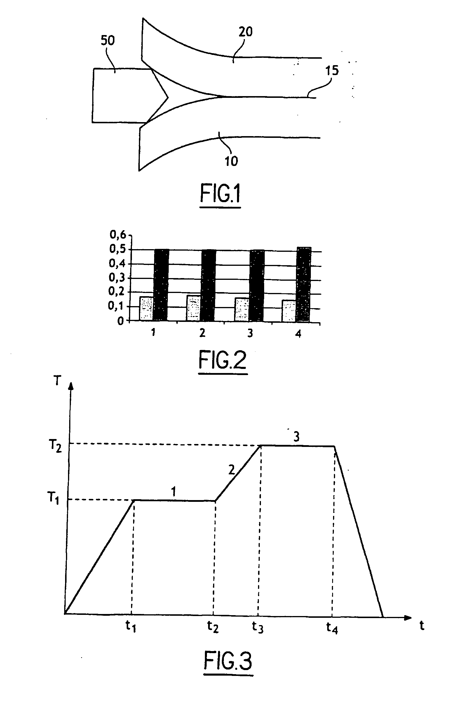
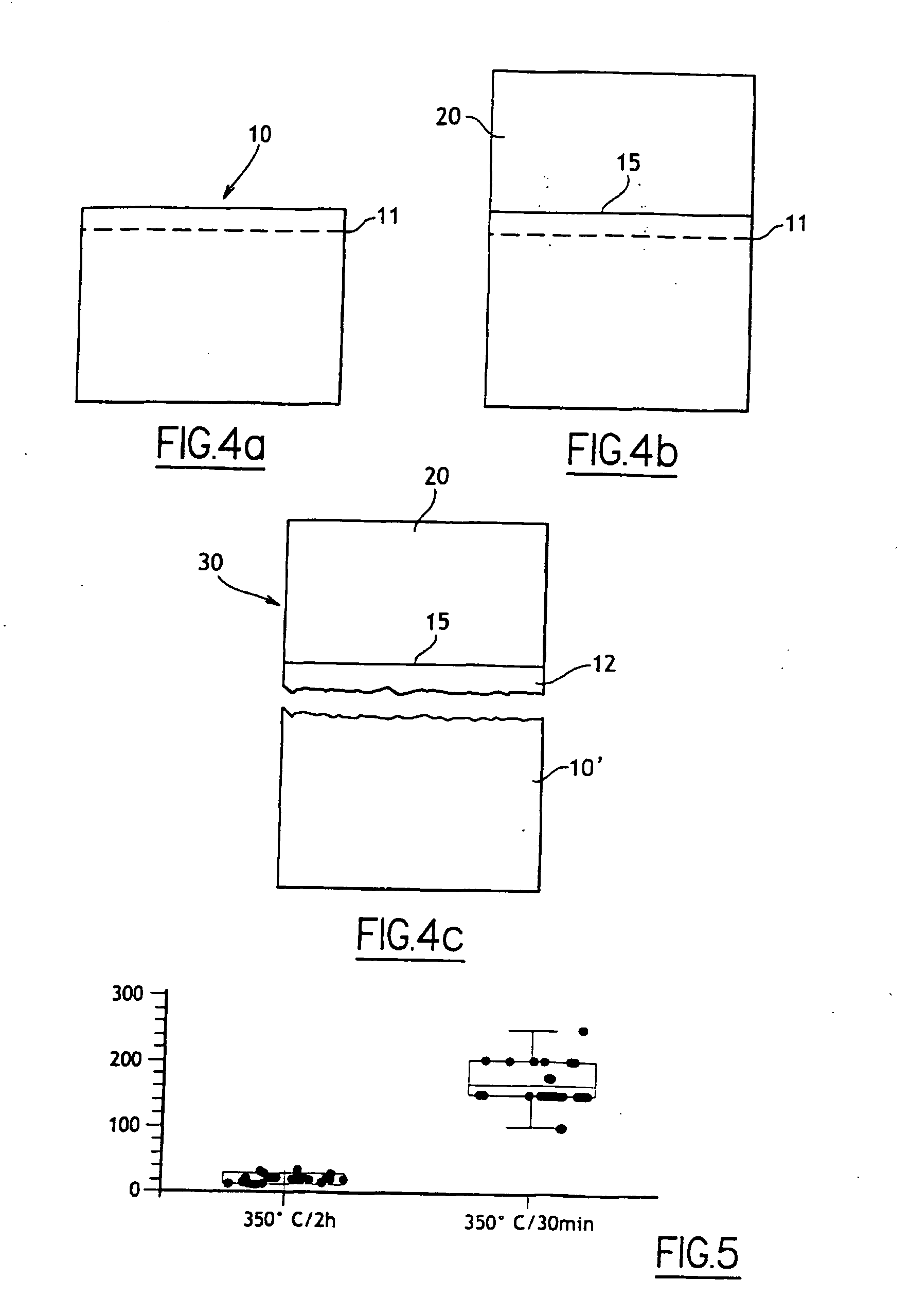
[0019] Generally, the present method seeks provide an improved method for transferring a useful layer from a first wafer to a second wafer, wherein the first wafer includes a zone of weakness that defines the useful layer. The useful layer is a semiconductor material. The technique includes bringing the surfaces of the two wafers into contact so that the surface of the useful layer is in contact with the second wafer, supplying heat energy at a first temperature that is substantially higher than ambient temperature for a first time period, and supplying additional heat energy to increase the temperature above the first temperature to detach the useful layer at the zone of weakness.

[0020] Preferred aspects of the bonding method may include any of the following features. Heat energy at a second temperature that is substantially higher than the first temperature may be applied for a second time period that follows the first application of heat, to reinforce the bonding linkages betwee...


PUM


Abstract

A method for minimizing defects when transferring a useful layer from a donor wafer to a receptor wafer is described. The method includes providing a donor wafer having a surface below which a zone of weakness is present to define a useful layer to be transferred, molecularly bonding at a bonding interface the surface of the useful layer of the donor wafer to a surface of the receptor wafer to form a structure, heating the structure at a first temperature that is substantially higher than ambient temperature for a first time period sufficient to liberate water molecules from the bonding interface, with the heating being insufficient to cause detachment of the useful layer at the zone of weakness, and detaching the useful layer from the donor wafer.

Description

BACKGROUND [0001] 1. Field of the Invention [0002] The present invention relates to methods for minimizing defects when transferring a useful layer of semiconductor material from a first wafer to a second wafer to produce a final structure. The final structure may be a semiconductor-on-insulator (SOI) structure that is useful for microelectronics, optics or optoelectronics applications. [0003] 2. Background Art [0004] A typical layer transfer process includes forming a zone of weakness in a first wafer at a depth that is close to or greater than the thickness of a transfer layer. The zone of weakness is created by implanting atomic species, or by forming a porous layer, or by using any other method to weaken the mechanical bonds at a predetermined depth in the first wafer. The layer transfer process also includes bringing the surfaces of the two wafers into contact so that a surface of the transfer layer is in contact with the second wafer, and then supplying energy to detach the tr...

Claims


Application Information

Patent Timeline
Patent Type & Authority Applications(United States)
IPC IPC(8): H01L21/30
CPCH01L21/76254H01L21/76251H01L27/12
Inventor BEN MOHAMED, NADIAMALEVILLE, CHRISTOPHEMAUNAND TUSSOT, CORINNE
Owner S O I TEC SILICON ON INSULATOR THECHNOLOGIES
Why Eureka
Try Eureka